Skip to main content Accessibility help
×
Hostname: page-component-77c89778f8-sh8wx Total loading time: 0 Render date: 2024-07-22T00:32:30.352Z Has data issue: false hasContentIssue false

7 - Basic gain stages

Published online by Cambridge University Press:  17 December 2010

Márcio Cherem Schneider
Affiliation:
Universidade Federal de Santa Catarina, Brazil
Carlos Galup-Montoro
Affiliation:
Universidade Federal de Santa Catarina, Brazil
Get access

Summary

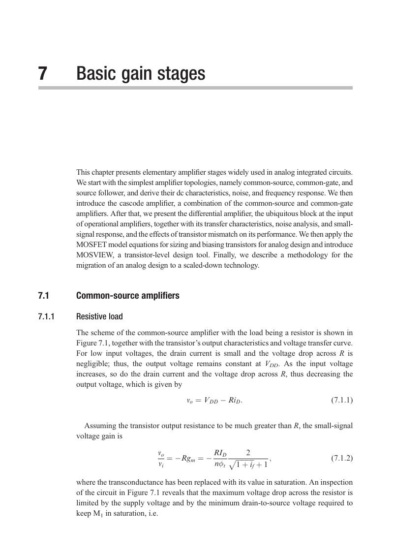
Image of the first page of this content. For PDF version, please use the ‘Save PDF’ preceeding this image.'
Type
Chapter
Information
Publisher: Cambridge University Press
Print publication year: 2010

Access options

Get access to the full version of this content by using one of the access options below. (Log in options will check for institutional or personal access. Content may require purchase if you do not have access.)

References

Gray, P. R., Hurst, P. J., Lewis, S. H., and Meyer, R. G., Analysis and Design of Analog Integrated Circuits, 4th edn., New York: John Wiley & Sons, 2001.Google Scholar
Silveira, F., Flandre, D., and Jespers, P. G. A., “A gm/ID based methodology for the design of CMOS analog circuits and its application to the synthesis of a silicon-on-insulator micropower OTA,” IEEE Journal of Solid-State Circuits, vol. 31, no. 9, pp. 1314–1319, Sep. 1996.CrossRefGoogle Scholar
Bult, K. and Blauschild, R., “CMOS op-amp design,” Advanced Engineering Course on Transistor-Level Analog IC Design, Lausanne, EPFL, Oct. 2002.Google Scholar
Horowitz, P. and Hill, W., The Art of Electronics, 2nd edn., Cambridge: Cambridge University Press, 1989.Google Scholar
Vittoz, E., “Micropower techniques,” in Design of Analog-Digital VLSI Circuits for Telecommunications and Signal Processing, 2nd edn., ed. Franca, J. E. and Tsividis, Y., Englewood Cliffs, NJ: Prentice-Hall, 1994, pp. 53–96.Google Scholar
Grebene, A. B., Bipolar and MOS Analog Integrated Circuit Design, Hoboken, NJ: Wiley Interscience, 2003.Google Scholar
Johns, D. A. and Martin, K., Analog Integrated Circuit Design, New York: Wiley, 1997.Google Scholar
Vincence, V. C., Galup-Montoro, C., and Schneider, M. C., “A high-swing MOS cascode bias circuit,” IEEE Transactions on Circuits and Systems II, vol. 47, no. 11, pp. 1325–1328, Nov. 2000.Google Scholar
Aguirre, P. and Silveira, F., “Bias circuit design for low-voltage cascode transistors,” Proceedings of SBCCI 2006, pp. 94–98, Sep. 2006.Google Scholar
Bult, K. and Geelen, G. J. G. M., “A fast-settling CMOS op amp for SC circuits with 90-dB DC gain,” IEEE Journal of Solid-State Circuits, vol. 25, no. 6, pp. 1379–1384, Dec. 1990.CrossRefGoogle Scholar
Hosticka, B. J., “Improvement of the gain of MOS amplifiers,” IEEE Journal of Solid-State Circuits, vol. 14, no. 6, pp. 1111–1114, Dec. 1979.CrossRefGoogle Scholar
Säckinger, E. and Guggenbühl, W., “A high-swing, high-impedance MOS cascode circuit,” IEEE Journal of Solid-State Circuits, vol. 25, no. 1, pp. 289–298, Feb. 1990.CrossRefGoogle Scholar
Yang, H. C. and Allstot, D. J., “An active-feedback cascode current source,” IEEE Transactions on Circuits and Systems., vol. 37, no. 5, pp. 644–646, May 1990.CrossRefGoogle Scholar
Vittoz, E., “Elementary building blocks,” in Intensive Summer Course on CMOS VLSI Design: Analog & Digital, Lausanne, 1989.Google Scholar
Laker, K. R. and Sansen, W. M. C., Design of Analog Integrated Circuits and Systems, New York: McGraw-Hill, 1994.Google Scholar
Allen, P. E. and Holberg, Douglas R., CMOS Analog Circuit Design, 2nd edn., New York: Oxford University Press, 2002.Google Scholar
Razavi, B., Design of Analog CMOS Integrated Circuits, Boston, MA: McGraw-Hill, 2001.Google Scholar
Kamath, B. Y., Meyer, R. G., and Gray, P. R., “Relationship between frequency response and settling time of operational amplifiers,” IEEE Journal of Solid-State Circuits, vol. 9, no. 6, pp. 347–352, Dec. 1974.CrossRefGoogle Scholar
Palmisano, G. and Palumbo, G., “Analysis and compensation of two-pole amplifiers with a pole-zero doublet,” IEEE Transactions on Circuits and Systems I, vol. 46, no. 7, pp. 864–868, July 1999.CrossRefGoogle Scholar
Gray, P. R. and Meyer, R. G., “MOS operational amplifier design – a tutorial overview,” IEEE Journal of Solid-State Circuits, vol. 17, no. 6, pp. 969–982, Dec. 1982.CrossRefGoogle Scholar
Steyaert, M. S. J. and Sansen, W., “Power supply rejection ratio in operational transconductance amplifiers,” IEEE Transactions on Circuits and Systems, vol. 37, no. 9, pp. 1077–1084, Sep. 1990.CrossRefGoogle Scholar
Dostal, J., Operational Amplifiers, 2nd edn., Boston, MA: Butterworth-Heinemann, 1993.Google Scholar
Cunha, A. I. A., Schneider, M. C., and Galup-Montoro, C., “An MOS transistor model for analog circuit design,” IEEE Journal of Solid-State Circuits, vol. 33, no. 10, pp. 1510–1519, Oct. 1998.CrossRefGoogle Scholar
Pinto, R. L. Oliveira, Cunha, A. I. A., Schneider, M. C., and Galup-Montoro, C., “An amplifier design methodology derived from a MOSFET current-based model,” Proceedings of IEEE ISCAS 1998, Monterey, CA, USA, pp. I–301–I-304, June 1998.Google Scholar
Pinto, R. L. O., Schneider, M. C., and Galup-Montoro, C., “Sizing of MOS transistors for amplifier design,” Proceedings of of IEEE ISCAS 2000, Geneva, vol. 4, pp. 185–188, May 2000.Google Scholar
Binkley, D. M., Hopper, C. E., Tucker, S. D., et al., “A CAD methodology for optimizing transistor current and sizing in analog CMOS design,” IEEE Transactions on Computer-Aided Design, vol. 22, no. 2, pp. 225–237, Feb. 2003.CrossRefGoogle Scholar
Giacomelli, P., Schneider, M. C., and Galup-Montoro, C., “MOSVIEW: a graphical tool for MOS analog design,” 2003 International Conference on Microelectronic Systems Education, pp. 43–44, May 2003.Google Scholar
Giacomelli, P., Machado, C. R., Schneider, M. C., and Galup-Montoro, C., MOSVIEW: a graphical tool for MOS analog design, http://www.eel.ufsc.br/lci/mosview.
Galup-Montoro, C., Schneider, M. C., and Coitinho, R. M., “Resizing rules for MOS analog-design reuse,” IEEE Design & Test of Computers, vol. 19, no. 2, pp. 50–58, Mar.–Apr. 2002.CrossRefGoogle Scholar
Vittoz, E. A., “Future of analog in the VLSI environment”, Proceedings of IEEE ISCAS, pp. 1372–1375, 1990.Google Scholar
Ng, H.-T., Ziazadeh, R. M., and Allstot, D. J., “A multistage amplifier technique with embedded frequency compensation”, IEEE Journal of Solid-State Circuits, vol. 34, no. 3, pp. 339–347, Mar. 1999.Google Scholar
Nauta, B., “Analog CMOS low-power design considerations,” Digest of Technical Papers of “Low power-low voltage workshop” at ESSCIRC' 96, 1996.
Wu, Y., Ding, W., Ismail, M., and Olsson, H., “RF bandpass filter design based on CMOS active inductors,” IEEE Transactions on Circuits and Systems II, vol. 50, no. 12, pp. 942–949, Dec. 2003.CrossRefGoogle Scholar

Save book to Kindle

To save this book to your Kindle, first ensure coreplatform@cambridge.org is added to your Approved Personal Document E-mail List under your Personal Document Settings on the Manage Your Content and Devices page of your Amazon account. Then enter the ‘name’ part of your Kindle email address below. Find out more about saving to your Kindle.

Note you can select to save to either the @free.kindle.com or @kindle.com variations. ‘@free.kindle.com’ emails are free but can only be saved to your device when it is connected to wi-fi. ‘@kindle.com’ emails can be delivered even when you are not connected to wi-fi, but note that service fees apply.

Find out more about the Kindle Personal Document Service.

  • Basic gain stages
  • Márcio Cherem Schneider, Universidade Federal de Santa Catarina, Brazil, Carlos Galup-Montoro, Universidade Federal de Santa Catarina, Brazil
  • Book: CMOS Analog Design Using All-Region MOSFET Modeling
  • Online publication: 17 December 2010
  • Chapter DOI: https://doi.org/10.1017/CBO9780511803840.008
Available formats
×

Save book to Dropbox

To save content items to your account, please confirm that you agree to abide by our usage policies. If this is the first time you use this feature, you will be asked to authorise Cambridge Core to connect with your account. Find out more about saving content to Dropbox.

  • Basic gain stages
  • Márcio Cherem Schneider, Universidade Federal de Santa Catarina, Brazil, Carlos Galup-Montoro, Universidade Federal de Santa Catarina, Brazil
  • Book: CMOS Analog Design Using All-Region MOSFET Modeling
  • Online publication: 17 December 2010
  • Chapter DOI: https://doi.org/10.1017/CBO9780511803840.008
Available formats
×

Save book to Google Drive

To save content items to your account, please confirm that you agree to abide by our usage policies. If this is the first time you use this feature, you will be asked to authorise Cambridge Core to connect with your account. Find out more about saving content to Google Drive.

  • Basic gain stages
  • Márcio Cherem Schneider, Universidade Federal de Santa Catarina, Brazil, Carlos Galup-Montoro, Universidade Federal de Santa Catarina, Brazil
  • Book: CMOS Analog Design Using All-Region MOSFET Modeling
  • Online publication: 17 December 2010
  • Chapter DOI: https://doi.org/10.1017/CBO9780511803840.008
Available formats
×