
I. INTRODUCTION
Analog and radio frequency (RF) circuits play an essential role in bridging the physical and digital worlds. Data communication, for example, requires analog circuits to transform digital signals into electromagnetic waves or electrical pulses to enable data exchange through air or cables. The transformation between digital and physical signals is getting more and more demanding because the emerging trends of Big Data, Cloud Service, and Internet of Things (IoT) are driving up the amount of data communication exponentially. For example, to meet the rapidly growing demands on high-data rate communications, the IMT-2020 (5G) Promotion Group is targeting future 5G networks to support up to 20 gigabits-per-second (Gbps) [1], which is 20 times faster than the 1 Gbps specification for 4G. The increased bandwidth in data centers also speeds the adoption of 100 Gbps interconnects, which is 10 times faster than current 10 Gbps systems. At such enhanced data rates, it is still imperative to achieve higher power efficiency for the huge amount of data to transfer.
Complementary metal-oxide-semiconductor (CMOS) devices in advanced technologies have demonstrated significant improvement in speed and power achieved by scaling and low-voltage operation. However, the performance of analog/RF circuits is usually constrained by physical limitations; therefore, circuit designers still need to increase device channel length, raise supply voltages, or use off-chip devices to overcome circuit imperfections, such as mismatch, nonlinearity, noise, finite gain, and variation over process, voltage, and temperature (PVT). Besides, the deteriorated routing parasitics and strict layout rules often result in an enlarged design area. These effects diminish the benefits of device scaling and come with higher cost for analog/RF circuits.
Still, there are new opportunities. Interfaces between physical and digital worlds inherently contain three elements: analog/RF circuits, signal processing algorithms, and digital logic. As such, circuit imperfections can be tackled in the analog domain and also by signal processing techniques or digital logic. This digitally-assisted or signal processing-aided design strategy receives significant interest because it simplifies analog/RF circuits and improves overall speed and power efficiency in advanced technologies. Still, the optimal solution relies on a balance in complexity between analog and digital circuit implementations. As the balance varies with design target and process nodes, it is crucial for designers to have a good understanding of both circuit behavior and signal processing concepts so that a reasonable overhead can lead to major breakthroughs in overall performance.
This paper demonstrates the above mentioned concepts by providing a review of signal processing techniques that are commonly deployed in modern data communication circuits. This review covers several critical topics in wireless communications and wired data links. In Section II, digital pre- and post-calibrations for nonlinearity and mismatch in RF circuits is presented, as well as the signal processing-aided design of high-resolution A/D converters (ADCs). Section III introduces equalization techniques for non-ideal channels in wired data links and background calibration techniques for channel mismatch in time-interleaved ADCs. These examples demonstrate that simple signal processing concepts can be very effective in solving design bottlenecks. As device scaling continues, more complex digital signal processing (DSP) will become feasible to further simplify analog/RF circuits. These and other future perspectives are discussed in Section IV.
II. SIGNAL PROCESSING IN WIRELESS COMMUNICATIONS
With the trend towards fully integrated, low-cost wireless transceivers, the conventional superheterodyne architecture [Reference Razavi2], which performs partial channel selection at progressively lower center frequencies and requires several bulky off-chip filters, is being supplanted by the direct-conversion architecture [Reference Abidi3,Reference Razavi4]. Direct conversion utilizes quadrature modulation to translate the desired signal directly up/down between the carrier and baseband frequencies, and therefore, eliminates all off-chip filters. It is a superior architecture from a system-on-chip (SoC) integration point of view but suffers from multiple circuit impairments, such as I/Q mismatch, intermodulation, DC offset, etc. These impairments may result in signal-to-noise ratio (SNR) degradation in the desired channel or leakage power to other channels. While the recent explosive growth in uplink and downlink carrier aggregation in long term evolution (LTE) networks leads to simultaneously receiving and transmitting in multiple bands and more complicated combinations of signal channels, the concepts of digitally-assisted calibration and signal processing-aided design become increasingly important to overcome the impairments in various scenarios. In this section, the examples of image rejection for I/Q mismatch, digital pre-distortion (DPD) for PA non-linearity, and ΔΣ modulation for high-resolution A/D conversion are presented.
A) I/Q mismatch and image rejection
1) Frequency-independent (FI) I/Q mismatch calibration
Figure 1 shows a direct-conversion transceiver. In the receiver, the RF signal is down-converted by complex mixing with two versions of the local oscillator (LO) signals, cos(ω LO t) and -sin(ω LO t), having a phase difference of 90°. The principle of quadrature modulation can be understood by its output
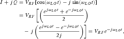 $$\eqalign{I + jQ & = V_{RF} [\cos (\omega_{LO} t) - j \sin (\omega_{LO} t)] \cr & = V_{RF} \left[\left({e^{j\omega_{LO} t} + e^{-j\omega_{LO}t} \over 2} \right) \right. \cr &\quad -\left. j \left( {e^{j\omega_{LO} t} - e^{-j\omega_{LO} t} \over 2j} \right) \right] = V_{RF} e^{-j\omega _{LO} t},}$$
which is the convolution of the RF signal and a single impulse at −ω
LO
. Figure 2 illustrates the desired channel being shifted from the carrier frequency directly to
 $\omega_{RF}-\omega_{LO}$
around DC, and consequently, the channel selection filter can be implemented at baseband using on-chip low-pass filters (LPFs) with very sharp roll off.
$\omega_{RF}-\omega_{LO}$
around DC, and consequently, the channel selection filter can be implemented at baseband using on-chip low-pass filters (LPFs) with very sharp roll off.

Fig. 1. Direct-conversion: (a) receiver architecture and (b) transmitter architecture.

Fig. 2. Principle of quadrature modulation in direct-conversion receiver.
It is noted that mismatch between the quadrature branches would result in incomplete cancellation of the e jω t terms in equation (1). This problem is especially critical in direct conversion because the device sizes in the mixers and LOs are reduced to allow operation at the RF carrier frequency, resulting in increased mismatch between the I and Q branches. I/Q mismatch can cause problems both in receivers and transmitters, as shown in Figs 3(a) and 3(b), respectively. In receivers, the image at −ω RF is translated to baseband by the residual impulse at e jω t , corrupting the desired signal [Reference Liu5]. In transmitters, I/Q mismatch results in the deviation of the constellation points from their ideal locations and thus degrades the error vector magnitude (EVM) and bit error rate (BER) [Reference Hieu, Ryu, Wang and Chen6].

Fig. 3. (a) Image at receiver output, and (b) EVM degradation at transmitter output due to I/Q mismatch.
In direct-conversion receivers, DSP can be applied to remove the residual image after A/D conversion [Reference Sohn, Jeong and Lee7,Reference Pun, Franca and Azeredo-Leme8]. Figure 4 shows an equivalent model of the quadrature mixer with a gain mismatch, ε, and a phase mismatch, θ, as well as the corresponding digital calibration functions. Assume first that ε and θ are frequency independent. Since the output signal, I′+jQ′, contains the desired signal, I+jQ, and its image, I−jQ, it can be observed that I′ and Q′ are each composed of both ideal I and Q as follows
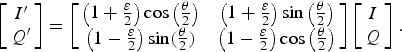 $$\left[\matrix{I^{\prime} \cr Q^{\prime}} \right] = \left[\matrix{\left( 1 + {\varepsilon \over 2} \right) \cos \left({\theta \over 2} \right) &\left(1 + {\varepsilon \over 2} \right) \sin \left({\theta \over 2} \right)\cr \left(1 - {\varepsilon \over 2} \right) \sin \lpar {\theta \over 2} \rpar & \left(1 - {\varepsilon \over 2} \right) \cos \left({\theta \over 2} \right)} \right] \left[\matrix{I \cr Q} \right].$$
Given this, the mismatch between the two branches can be corrected digitally using a compensation matrix to reconstruct the original I and Q from I ′ and Q ′, as shown in the implementation in Fig. 4, where
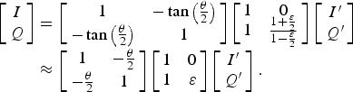 $$\eqalign{\left[\matrix{I \cr Q} \right] & =\left[\matrix{1 & -\tan \left({\theta \over 2} \right) \cr -\tan \left({\theta \over 2} \right) & 1} \right] \left[\matrix{1 & 0 \cr 1 & {1 + {\varepsilon \over 2} \over 1 - {\varepsilon \over 2}}} \right] \left[\matrix{I^{\prime} \cr Q^{\prime}} \right] \cr &\approx \left[\matrix{1 & -{\theta \over 2} \cr - {\theta \over 2} & 1} \right] \left[\matrix{1 & 0 \cr 1 & \varepsilon} \right] \left[\matrix{I^{\prime} \cr Q^{\prime}} \right].}$$
The values of ε and θ can be found by simply applying a test tone to the receiver input before normal operation. Intuitively, the gain mismatch, ε, is proportional to the output power ratio of I′ and Q′, and the product of I′ and Q′ would reveal the phase mismatch, θ, since ideal I and Q are orthogonal with zero dot product:
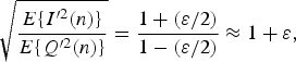 $$\eqalign{\sqrt{{E\{I^{\prime 2}(n)\} \over E\{Q^{\prime 2}(n)\}}} &= {1 + (\varepsilon /2) \over 1 - (\varepsilon /2)} \approx 1 + \varepsilon,}$$
 $$\eqalign{{2E\{I^{\prime} (n)Q^{\prime} (n)\} \over E\{I^{\prime 2}(n)\} + E\{Q^{\prime 2}(n)\}} &= {1-(\varepsilon^2 /4) \over 1 + (\varepsilon^2 /4)} \sin \theta \approx \tan \theta,}$$
where E{·} is the expectation operator. As discussed in Section I, the idea of digitally-assisted techniques is to balance the complexity in analog and digital circuit implementations. The approximations in equations (4) and (5) reduce the complexity of digital logic, relying on small enough ε and θ in the analog circuits.

Fig. 4. Behavior model of FI I/Q mismatch in quadrature mixer and digital compensation functions.
Figure 5 shows simulated results with practical ε and θ values. It demonstrates that image rejection ratio (IRR) is improved from 22 to 61 dB after digital calibration. The calibration takes around 100 μs and is performed when the system starts up. This off-line calibration is not able to track the variation of I/Q mismatch due to temperature drift; however, a practical estimation is that the IRR may degrade from >45 dB to slightly below 40 dB over temperature. This is good enough for most applications, but for advanced modulation schemes requiring SNR higher than 40 dB, such as 1024 quadrature amplitude modulation (QAM), compensation for temperature drift becomes necessary. This results in the increasing demand for background I/Q mismatch calibration in high-data rate communications to update ε and θ without interrupting system's normal operation.

Fig. 5. Simulated IRR before and after I/Q mismatch calibration.
2) Frequency-dependent (FD) I/Q mismatch calibration
The assumption of FI I/Q mismatch is valid in most receivers so long as the mixers, amplifiers, filters, and data converters have wide bandwidth compared with the desired channel such that the variation within a limited frequency range is negligible. However, FD mismatch is becoming significant in high-data rate wireless systems with increased channel bandwidth, e.g., IEEE 802.11ac [9]. In 802.11ac, the use of high-order modulation, such as 256-QAM, demands at least 40-dB IRR to ensure sufficient SNR in each sub-carrier. In such a case, the calibration of FD I/Q mismatch [Reference Valkama, Renfors and Koivunen10] is becoming necessary.
FD I/Q mismatch arises due to the different frequency responses between analog I/Q branches. Figure 6 models this mismatch using two filters with different frequency responses, H I (f) and H Q (f), for the I and Q branches, respectively. To analyze the effect of FD I/Q mismatch, assume first for simplicity that there is no FI I/Q mismatch. In this case, the quadrature signal can be represented as
 $$\eqalign{I^{\prime} + jQ^{\prime} &= H_I (f)I + jH_Q (f)Q \cr &= {H_I (f)+H_Q (f) \over 2}(I + jQ) \cr &\quad + {H_I (f)-H_Q (f) \over 2}(I - jQ).}$$
As shown in equation (6), the difference between H I (f) and H Q (f) results in an non-zero image component of I−jQ along with the signal I+jQ. Therefore, FD I/Q mismatch contaminates the desired signal by the image.

Fig. 6. Digital compensation of FD I/Q mismatch.
Since I/Q mismatch can be modeled in the baseband, digital compensation techniques are popularly used to estimate and compensate for this mismatch. That is, the difference of analog I/Q responses can be counteracted by a digital filter having frequency response of H I (f)/H Q (f) [Reference Xing, Shen and Liu11]. In a system with minor FD I/Q mismatch, H I (f)/H Q (f) is relatively flat across frequencies. In the time domain, this corresponds to a short impulse response, and it is reasonable to approximate H I (f)/H Q (f) with a digital finite impulse response (FIR) filter. Figure 6 also illustrates the implementation of the above mentioned compensation. The FIR filter ω(n) in the Q branch is meant for compensating for the FD I/Q mismatch. The delay block in the I branch matches the delay introduced by ω(n). The coefficients of the FIR filter can be found by applying test tones at different frequencies to detect the FD mismatch.
For practical systems having both FI and FD I/Q imbalances, the compensation schemes depicted in Figs 4 and 6 are used in tandem. Although the block diagram of FD I/Q mismatch compensation in Fig. 6 seems simple, in practice, a large number of taps may be required in the filter, increasing the number of multipliers needed. As the IRR requirement and signal bandwidth increases, the hardware cost for long word length and the power dissipated at high sampling frequency should be well considered.
B) Intermodulation and DPD for power amplifiers (PAs)
Nonlinearity, which modulates the signal and interferers to different frequencies, is another major concern in RF circuits. One scenario of interest occurs when two interferers at ω1 and ω2 are located nearby the desired channel, as depicted in Fig. 7(a). If the nonlinear system has an input/output characteristic of y(t)=x(t)+α3 x(t)Reference Abidi 3 and assuming x(t)=A 1cos(ω1 t)+A 2cos(ω2 t), the output becomes
 $$\eqalign{y(t) & =[A_1 \cos (\omega _1 t) + A_2 \cos (\omega_2 t)]\cr &\quad + \alpha_3 [A_1 \cos (\omega_1 t) + A_2 \cos (\omega_2 t)]^3.}$$
The right-hand side of y(t) after expansion contains a dc component and harmonics, as well as 3rd-order intermodulation (IM3) products at 2ω1±ω2 and 2ω2±ω1. Figure 7(a) illustrates the case where the IM3 product at 2ω1−ω2 overlaps the desired channel and thus degrades the SNR. In wireless receivers, the nonlinearity is usually controlled by scaling the signal swing within the linear range of the circuits and leads to a fundamental tradeoff between linearity and noise performance of the receiver design.

Fig. 7. (a) 3rd-order intermodulation of interferers, and (b) spectral regrowth after power amplifier caused by nonlinearity.
In wireless transmitters, if the output swing of the PA is limited within the linear range, huge energy is wasted through the unused voltage headroom at large output current, where wasted power is equivalent to the voltage headroom multiplied by the current. Since the PA usually dominates the power consumption of the overall transceiver, enhancing PA efficiency by maximizing output swing is crucial. In such a case, even higher-order intermodulation products, such as IM5, may appear, resulting in leakage power at adjacent channels. Figure 7(b) shows this effect and the orthogonal frequency division multiplexing (OFDM) signal at the nonlinear PA output. The high leakage power to adjacent channels, called spectral regrowth, cannot be suppressed by the front-end band-pass filter and must be made small enough. To meet both power efficiency and linearity requirements, look-up tables (LUTs) in the digital baseband can be used to pre-distort the input signal and to compensate for the nonlinear PA behavior [Reference Kim and Konstantinou12, Reference Ding13].
Figure 8 explains the concept of DPD, which turns the nonlinear behavior of a transmitter into a linear function depicted by the dashed line. If the digital input applied to the baseband DAC is D 1, the amplitude at the PA output is V 1. To shift the amplitude from V 1 to V 1′ on the dashed line, a digital input of D 1′ should be applied to replace D 1. That is, if the input code D 1 is mapped to D 1′ in advance, the nonlinear PA behaves as a linear one. To apply this concept across the full range, a LUT can be used to “pre-distort” the digital input.

Fig. 8. Principle of DPD in power amplifier.
In practice, two LUTs are required, since a PA contains storage elements, and therefore, its amplitude variation results in both amplitude deviation (AM–AM conversion) and phase deviation (AM–PM conversion) [Reference Ku and Kenney14]. To illustrate this, assume for simplicity that both amplitude and phase deviation are frequency independent, the input of the PA is V i (t)e jθi(t), and its output is V o (t)e jθ o(Vi(t)). AM–AM conversion and AM–PM conversion occur as follows
 $$\eqalign{AM - AM &= {V_o (t) \over V_i (t)} \cr AM - PM & = {\theta_o [V_i (t)] \over \theta _i (t)}.}$$
Figure 9 shows the calibration scheme used to obtain the LUT values, in which a ramp signal is applied at the digital baseband of the transmitter. The slow ramp signal is up-converted to RF frequency and down-converted by the receiver. The PA distortion at different ramp amplitudes is digitized by the receiver ADC. After rate conversion and averaging to remove circuit noise, a least mean squares (LMS) search block updates the values in the two LUTs to minimize the difference between the original and received ramp signals [Reference Muhonen, Kavehrad and Krishnamoorthy15]. Figure 10 shows measured results before and after calibration. It demonstrates that the leakage power at adjacent channels is reduced around 10 dB after DPD.

Fig. 9. DPD by LUT and LMS search.

Fig. 10. Measured OFDM spectrum before and after DPD.
This calibration scheme is quite straight forward because it assumes the AM–AM and AM–PM conversions are memory-less, which means the amplitude and phase deviations are not affected by the previous symbols and remain constant for the same digital input. Although it is possible to perform DPD with memory effect, it would be much more complicated than reducing the memory effect in the circuits. This calibration, performed during system start-up, takes around 100 ms and also suffers from temperature drift. To maintain an acceptable EVM over temperature, the PA needs to be designed to allow temperature drift by sacrificing the efficiency. Therefore, background DPD is also becoming the clear trend to maximize PA power efficiency in order to meet the continuing demand for low-power systems.
C) BasebandΔ Σ A/D converter
In a modern wireless receiver, direct conversion eases the design of the channel selection filter at baseband. It remains difficult, however, to remove interferers located immediately adjacent to the desired channel without significant power and area cost in analog filters. In practice, the input of the baseband ADC may still receive huge adjacent channel interferers, leading to an ADC with wide input range and fine quantization steps to digitize the desired signal with sufficient SNR. In cellular communications, ADCs with resolution higher than 12 bits are typically required. At these resolutions, multiple components in conventional ADC architectures are seriously affected by circuit imperfections, and consequently, the power and area grow exponentially for every extra bit of resolution. To avoid the demand for high-precision components, signal processing can be incorporated into the ADC design, called ΔΣ modulation [Reference Schreier, Temes and Norsworthy16], which allows high-resolution A/D conversion to be realized with low-resolution ADCs, such as a 1-bit quantizer.
1) Δ Σ A/D converter
Figure 11 illustrates the architecture and behavior of an ΔΣ ADC, which utilizes “oversampling” and “noise shaping” to spread the noise over a wide bandwidth and to shift quantization error to higher frequencies, respectively, so that a high in-band SNR can be achieved. The ΔΣ modulator contains an integrator, L(z), and a low-resolution ADC within a negative feedback loop, where Δ and Σ refer to the negative feedback and the integrator, respectively. The modulator output, Y, can be represented by its input, X, plus the quantization error, Q, as
 $$Y = {L(z) \over 1 + L(z)} X + {1 \over 1 + L(z)}Q.$$
Equation (9) implies that when L(z) is very large, Y is equivalent to X because the error term, 1/(1+L(z))Q, is almost zero. Figure 11 also shows the spectrum at the modulator output. Since L(z) is an integrator with high gain at DC, the quantization error within the desired channel is suppressed. After digital decimation filtering, a high-precision digital output is obtained, and any remaining adjacent channel interferers can be easily removed by further digital filtering.

Fig. 11. Principle of Δ Σ A/D conversion.
2) Continuous-time (CT) Δ Σ modulator
The integrator of a ΔΣ modulator can be a discrete-time (DT) filter, L(z), or a CT filter, L(s), as shown in Fig. 12. The CT implementation is usually preferred for its high power efficiency when signal bandwidths are >10 MHz. It does not rely on fast settling in DT filters and has an additional benefit of implicit anti-aliasing to simplify the preceding baseband filter. However, the modulator loop contains both CT and DT components and is too complex for circuit designers to analyze mathematically, especially with irregular DAC pulse shapes [Reference Oliaei17,Reference Ortmanns, Gerfers and Manoli18] and circuit non-idealities varying with PVT. The CT and DT mixed behavior eventually leads to numerous time-consuming iterations before reaching a proper design. Nevertheless, this issue can be tackled by curve fitting with least squares method [Reference Schreier, Temes and Norsworthy16], which also enables the opportunity to compensate for finite operational amplifier bandwidth by optimizing system coefficients. This allows the design requirements to be further relaxed, leading to significant power savings [Reference Ortmanns, Gerfers and Manoli19].

Fig. 12. CT versus DT Δ Σ modulator.
The design methodology of a CT modulator is essentially to match its DT counterpart, or more specifically, for the same ADC output sequence D(n) in Fig. 12, the same values of V(n) should be sampled at the ADC input. This requirement can be seen as matching the impulse response of a CT filter, L(s), with its DT equivalent, L(z), at every sampling point. Figure 13 shows the system model of a 3rd-order CT modulator, where
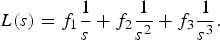 $$L(s) = f_1 {1 \over s} + f_2 {1 \over s^2} + f_3 {1 \over s^3}.$$
The impulse response of the loop, from the ADC output to the ADC input, is affected by the delay block, the DAC pulse shape, and the non-ideal integrators. For these effects, the model also includes an additional fast feedback path, f 4 z −1, to compensate for the excess loop delay in order to match L(z) properly [Reference Keller, Buhmann, Sauerbrey, Ortmanns and Manoli20]. Complex mathematics are avoided by finding the impulse responses of the 1st-order, 2nd-order, and 3rd-order paths directly based on circuit simulation as h 1(n), h 2(n), and h 3(n). Since the design target is to match the impulse response of the L(z), h L(z)(n), the optimal values for f 1, f 2, f 3, and f 4 can be obtained by solving the following equations using the least squares method.
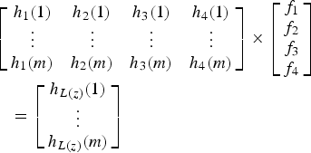 $$\eqalign{&\left[\matrix{h_1 (1) & h_2 (1) & h_3 (1) &h_4 (1) \cr \vdots & \vdots & \vdots & \vdots \cr h_1 (m) & h_2 (m) & h_3 (m) &h_4 (m)} \right] \times \left[\matrix{f_1 \cr f_2 \cr f_3 \cr f_4} \right]\cr &\quad =\left[\matrix{h_{L(z)} (1) \cr \vdots \cr h_{L(z)} (m)} \right]}$$
In equation (11), m is the number of impulse response samples to be considered. Theoretically, m=4 is enough, but due to circuit non-idealities, different settings of m may lead to different solutions. The optimal coefficients can be obtained with a proper choice of m depending on the characteristics of the design [Reference Pavan21].

Fig. 13. Principle of impulse response curve fitting for CT Δ Σ modulator design.
The principle behind this methodology is to compensate for the non-ideal circuit behaviors, which cannot be well defined, using system design approaches. For example, the required operational amplifier (OpAmp) bandwidths for the integrators can be relaxed from 2 to 3× the sampling frequency, f S , to 0.5–1× by adjusting the filter coefficients [Reference Shu, Tsai, Chen, Lo and Chiu22], as demonstrated in Fig. 14. Figures 14(a) and 14(b) are the simulated output spectrums of a 3rd-order DT modulator and its CT counterpart with ideal coefficients found by the conventional mathematical method. In this example, the OpAmp bandwidth can be relaxed to 3× f S without significant difference in the output spectrum. However, if the OpAmp bandwidth is further reduced to 1× f S , as depicted in Fig. 14(c), it degrades the phase margin of the loop as evident by the peaking shown in the output spectrum. This implies the modulator can easily become unstable with additional PVT variations. Nevertheless, once the compensation scheme is applied, the loop stability is recovered, as shown in Fig. 14(d). Since the OpAmps usually consume >60% of the total power, the compensation technique can easily gain >30% power saving together with enhanced tolerance on PVT variations. This is becoming important for carrier aggregation in LTE networks, where the power dissipated in the ADCs is becoming significant due to the high bandwidth requirement and the increased number of channels.

Fig. 14. Simulated output spectrums of (a) DT Δ Σ modulator, (b) ideal CT counterpart, (c) ideal CT counterpart with low-speed OpAmp, and (d) CT Δ Σ modulator with low-speed OpAmp after coefficient compensation.
III. SIGNAL PROCESSING IN WIRED DATA LINKS
In wired data communications, a pulse sequence, such as a non-return-to-zero (NRZ) pulse, is transmitted through a physical channel consisting of cables, connectors, printed-circuit-board routings, vias, and chip packages. The characteristics of the overall channel determine the signal quality at the receiver end, which suffers from distortion due to channel loss, reflection, and noise interference. As data rates climb higher, the bandwidth of a pulse sequence correspondingly increases. Therefore, the signal energy at high frequencies is inevitably attenuated by the low-pass channel response, which results in a poor SNR at the receiver end. Although cables with wide bandwidth can be used, it increases the cost. To overcome the imitation imposed by physical channels, various equalization techniques have been developed to restore the original pulse so as to reduce the BER and maximize the data rate [Reference Stojanovic23].
Equalization techniques involve signal processing in both analog and digital domains. Analog solutions tend to consume less power, but digital approaches provide flexibility to deal with complicated channel characteristics and modulation schemes. In advanced digital equalization architecture, high-speed ADCs are essential to digitize the signal at the receiver input. In the section, the signal processing techniques commonly used in the equalization schemes and the high-speed ADCs are presented.
A) Equalization technique in wired data links
Figure 15 shows a simplified wired communication system model with various equalization schemes. Also shown are the channel frequency response and impulse response. A typical channel frequency response exhibits a low-pass behavior with small bumps resulting from complex reflections of the non-continuous channel impedance. The corresponding impulse response contains both the pre- and post-cursor inter-symbol interference (ISI), which causes poor SNR at the receiver front-end as shown in the eye diagram at node A.

Fig. 15. Simplified model of wired data communication across physical channel.
The equalization schemes, including transmitter emphasis, linear equalizer (LE), and decision feedback equalizer (DFE), compensate for the pre- and post-cursor ISI in order to enhance the SNR and eye-opening before the slicer. The transmitter emphasis is typically a FIR filter with 2–3 taps to equalize one pre-cursor and an additional post-cursor ISI simultaneously. The LE is usually composed of an analog filter with a zero and a pole to remove the long decaying post-cursor ISI tail beyond the reach of the following DFE. The effectiveness of these two blocks is evident as shown in the eye diagram at the LE output (node B), where the eye-opening is clearly seen. To further enhance SNR for high data rate, DFE can be applied to enhance the SNR before slicer.
Figure 16 shows two types of DFE realized with either infinite impulse response (IIR) or FIR filters, where D refers to D flip-flop with unity delay. Both of them provide analog feedback to the slicer input. DFE with IIR filters [Reference Kim, Liu, Dickson, Bulzacchelli and Friedman24] is suitable for low-power applications since analog filters with proper pole (p 1, p 2) and gain (A 1, A 2) values are able to emulate and cancel a series of post-cursor ISI. This type of DFE performs well for channels with smooth frequency response, but does not deal well with bumps due to complex reflections. DFE with FIR filters feeds back binary levels through an FIR filter directly. Since each post-cursor ISI value is compensated for by an optimal tap weight (C 1, C 2) proportional to its amplitude, it is more flexible and works better for channels with bumpy frequency response.

Fig. 16. Decision feedback equalization with IIR and FIR filters.
In DFE, the most critical challenge is how to set the parameters in the IIR or FIR filters if the channel behavior remains unknown, especially when a training sequence is not applicable. Figure 17 demonstrates how the tap weights of a 4-tap FIR-filter DFE are optimized by a sign-sign LMS algorithm. In the bottom part of Fig. 17, the amplitude of the main cursor, C 0, is found by an additional slicer with variable threshold, where C 0 is the threshold when the additional slicer output exhibits equal numbers of 1 s and −1 s with a zero average. The error term, e(n), to be minimized by the LMS algorithm is then defined as the difference between the slicer input and output multiplied by C 0. The sign-sign LMS function updates the tap weights, C 1–C 4, according to the sign of e(n) with a step size, μ, as
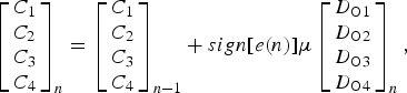 $$\left[\matrix{C_1 \cr C_2 \cr C_3 \cr C_4} \right]_n = \left[\matrix{C_1 \cr C_2 \cr C_3 \cr C_4} \right]_{n - 1} + sign[e(n)]\mu \left[\matrix{D_{{\rm O}1} \cr D_{{\rm O}2} \cr D_{{\rm O}3} \cr D_{{\rm O}4}} \right]_n,$$
where D 1–D 4 are consecutive slicer output samples. The eye diagram after DFE (node C) in Fig. 15 demonstrates that a wide eye-opening with optimized tap weights is achieved by the LMS algorithm.

Fig. 17. FIR-filter DFE with adaptive LMS algorithm.
B) Time-interleaved ADCs for wired data links
The communication links deployed in data centers have continued marching towards higher data rates. To increase the throughput of backplane links to 50 Gbps, the use of multi-level signals at lower baud rates, such as PAM-4 [Reference Zerbe25], offers the advantage of higher SNR at the receiver input compared with NRZ pulses. It increases the complexity of the receiver and leads to an emerging trend of ADC-based receivers, in which the signal is first digitized at the receiver input, and then passed through programmable LEs and DFEs implemented with DSP logic. This architecture requires high-speed, low-to-medium-resolution ADCs. For example, 10GBASE-T and 400 Gigabit Ethernet require 12-bit and 7-bit ADCs with sampling rates up to 0.8 and 25 GHz, respectively. These high-performance ADCs increase the system power dissipation and result in serious concern of heat dissipation due to the huge amount of data to transfer.
When the speed of an ADC is pushed to the limit imposed by process technology, it takes significant power to gain any minor improvement in speed [Reference Walden26] and comes with a cost of less tolerance to PVT variation. In such cases, the time-interleaved architecture [Reference Black and Hodges27], has become popular since it allows ADCs to extend their speed without significant degradation in power efficiency [Reference Kull28,Reference Jo29]. Figure 18 shows the architecture of a time-interleaved ADC, where the input samples are processed sequentially by N different channels. The speed of each ADC channel is relaxed by N times, and therefore, the power efficiency can be optimized. However, the channel mismatches in gain, offset, and sampling instant generate error patterns corresponding to the rotation of the N-channels. These mismatches need to be small enough over PVT variation to avoid SNR degradation, and consequently, signal processing techniques to detect mismatch errors without interrupting ADC's normal operation have generated significant interest recently [Reference Fu, Dyer, Lewis and Hurst30,Reference Jamal, Fu, Chang, Hurst and Lewis31].

Fig. 18. Architecture of time-interleaved ADC.
1) Estimation of gain and offset errors by pseudo-random pulse sequence
One of the mostly commonly used techniques for background calibration is to inject a pseudo-random test signal, which is not correlated to the desired signal. Figure 19(a) shows how the gain error of each channel is estimated by injecting a pseudo-random noise (PN) pulse sequence, {1,−1}, into the ADC input [Reference Siragusa and Galton32]. Assume that the ADC has a gain error, ε. The test signal, V CAL , is modulated by PN and added to the ADC input, V IN . The test signal is then digitized by the ADC along with the input signal. After correlating the ADC output digitally with the same PN, the output becomes
 $$V_{IN} (1 + \varepsilon) PN + V_{CAL} (1 + \varepsilon) PN^2.$$
By doing so, the input signal is modulated by PN and translated into noise. On the other hand, the PN-modulated calibration signal becomes a DC value of
 $(1 + \varepsilon) V_{CAL}$
since PN
2=1. The noise term of
$(1 + \varepsilon) V_{CAL}$
since PN
2=1. The noise term of
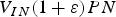 $V_{IN}(1+\varepsilon) PN$
is then removed by averaging the ADC output in order to extract (
$V_{IN}(1+\varepsilon) PN$
is then removed by averaging the ADC output in order to extract (
 $1 + \varepsilon)V_{CAL}$
. Ideally, this noise term approaches zero as more samples are averaged. Once (
$1 + \varepsilon)V_{CAL}$
. Ideally, this noise term approaches zero as more samples are averaged. Once (
 $1 + \varepsilon)V_{CAL}$
is obtained, the original output, (
$1 + \varepsilon)V_{CAL}$
is obtained, the original output, (
 $1 + \varepsilon)V_{IN}$
, is recovered by subtracting (
$1 + \varepsilon)V_{IN}$
, is recovered by subtracting (
 $1 + \varepsilon)V_{CAL}$
from the digital output.
$1 + \varepsilon)V_{CAL}$
from the digital output.

Fig. 19. (a) Estimation of gain error by PN injection, and (b) estimation of offset error by PN modulation.
Similar concept has been used to estimate the offset error [Reference Gulati and Lee33], as shown in Fig. 19(b). Assume first that the effect of device mismatch is grouped into a DC offset, V OFFSET , at the ADC input. By modulating the ADC input with PN, the ADC output becomes
 $$V_{IN} PN + V_{OFFSET} PN^2.$$
It shows that V IN is again randomized by PN, and its value approaches zero as a large number of output samples are averaged. After this measured offset is subtracted from the output, the original V IN can be restored by modulating the output with the same PN again.
2) Detection of sampling instant mismatch by correlation
The sampling instant mismatch refers to the delay mismatch in the sampling switches and control logic. Time-interleaved ADCs have previously been considered impractical because the solution for this issue is much more complicated than the PN injection for gain and offset errors. Recently, several solutions have been proposed [Reference Huang, Wang and Wu34–Reference Razavi36], and the time-interleaved architecture has become popular for high-speed A/D conversion. One of these solutions is based on digital correlation between the two interleaved channels [Reference Razavi36].
Figure 20 illustrates the fundamental principle of sampling error detection by correlation. For an input waveform, x, if the ideal sampling instant, T 1, is delayed by Δ T, the sampled signal contains an error term of Δ T(dx/dt), where dx/dt is the slope of the input waveform at T 1+Δ T/2. By correlating the digital output with dx/dt, the signal becomes
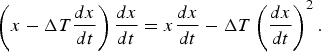 $$\left(x - \Delta T {dx \over dt} \right) {dx \over dt} = x {dx \over dt} - \Delta T \left({dx \over dt} \right)^2.$$
Since the signal, x, and its derivative, dx/dt, are orthogonal, the expected value of x(dx/dt) is zero. The polarity of Δ T can then be detected by averaging the right-hand side of equation (15) because (dx/dt)2 is always positive.

Fig. 20. Principle of sampling instant mismatch detection.
Figure 21 demonstrates how this concept is applied to two interleaved ADC channels, where channel 2 digitize x in equation (15) and channel 1 is used to find dx/dt for correlation. The target of this method is to align the sampling instants of channel 2 to the middle points of those in channel 1. The implementation involves multiplying the outputs of the two interleaved channels and taking the difference. The difference, D Δ T , becomes a measure of the sampling error of channel 2 [Reference Razavi36], where
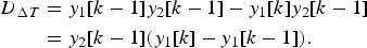 $$\eqalign{D_{\Delta T} &= y_1 [k - 1]y_2 [k - 1]-y_1 [k]y_2 [k-1] \cr &= y_2 [k - 1](y_1 [k] - y_1 [k - 1]).}$$
The result in equation (16) can be understood as the discrete-time counterpart of equation (15), where (x+ΔT dx/dt) is represented y 2[k−1], and the slope of dx/dt corresponds to y 1[k]−y 1[k−1] in equation (16).

Fig. 21. Detection of sampling instance mismatch by correlation.
A zero-forcing feedback loop can then be used to minimize the sampling error, D Δ T , according to its polarity. This calibration can be either in the digital domain using FIR filters [Reference Jamal, Fu, Chang, Hurst and Lewis31] or in the analog domain by tuning a variable-delay line for sampling instant. In [Reference Razavi36], the spurious tone caused by the sampling instant mismatch with a sinusoidal input is reduced from −52 dB to around −75 dB after the sampling instant tuning. The required tuning accuracy increases with the ADC resolution and the input signal bandwidth.
Since the equipments in data centers are seldom turned off, both the equalization techniques in wired data links and the calibration techniques for time-interleaved ADCs are performed during system's normal operation so as to track slow changes due to temperature drift or environmental variations.
IV. CONCLUSION
This paper has reviewed various signal processing techniques in wireless and wired data communication circuits. It demonstrates that devices with fundamental limitations on mismatch, nonlinearity, noise, and process variation, can still achieve high performance and high power efficiency with the assistance of signal processing algorithms, which can be in either the analog or digital domains. As Moore's Law continues, it is predicted that there will be more complex DSP and less complicated analog/RF circuits. Evidence of this vision can already be seen in the increasing number of analog/RF designs with extremely simplified architecture working in a digital manner, such as digital PAs, all-digital phase-locked loops, inverter-based operational amplifiers, and mostly-digital ADCs. There have also been attempts to make analog/RF circuit design more digital-like through the use of synthesizable “analog” standard cells. As the boundaries between analog circuits, digital logic, and signal processing algorithms continue to be blurred, designers will need to have a good understanding of all three domains, leading to more challenges, but also to more opportunities for future analog/RF circuit design.
ACKNOWLEDGEMENT
The authors would like to express sincere gratitude to the reviewers for the constructive suggestions that greatly improved the manuscript and also to our colleagues Yan-Bin Luo, Paul Liang, Jing-Hong C. Zhan, Guang-Kaai Dehng, Chih-Ming Hung, and Zoran Zvonar for their helpful advices and technical discussions.
Yun-Shiang Shu has been with MediaTek Inc., HsinChu, Taiwan, since 2010, where he is currently a Senior Project Manager. His works have been in the area of A/D and D/A data converters, digital techniques to compensate for analog circuit imperfections, and sensor readout interfaces. At MediaTek, he introduced multiple DSP-assisted ADC designs into mobile communication, wireless connectivity, and sensor readout product lines, contributing to substantial power and area saving. He is currently leading the development of analog front-ends for biomedical and IOT applications. Dr. Shu received the B.S. and M.S. degrees in Electrical Engineering from National Taiwan University, Taipei, Taiwan, in 1997 and 1999, respectively, and the Ph.D. degree in Electrical and Computer Engineering from University of California at San Diego in 2008. He is the first author of more than 10 technical papers in ISSCC, JSSC, VLSI, and CICC, covering the innovations of signal processing techniques for various types of ADCs. He currently serves as a Technical Program Committee member of the IEEE Symposium on VLSI Circuits.
Stacy Ho received the B.S. and M.S. degrees in Electrical Engineering from the Massachusetts Institute of Technology, Cambridge, MA, in 1992. From 1992 to 2001 he was with the High Speed Converter Group of Analog Devices, Wilmington, MA, where he designed high-speed CMOS pipeline ADCs for imaging and communication systems. In 2001, he joined the Communications Division of Analog Devices, where he designed the first GSM/EDGE RFCMOS front-end at ADI. He also designed baseband circuits, including channel select filters, Rx ADC, Tx DAC, and voltage regulators. Since 2008, he has been with MediaTek USA, Inc., Woburn, MA, where he is currently Deputy Technical Director leading the development of advanced data converters for wireless communications. Stacy has presented papers at the IEEE VLSI Circuits Symposium and the IEEE Radio Frequency Integrated Circuits Symposium (RFIC) and has co-authored papers at both the IEEE International Solid-State Circuits Conference (ISSCC) and at the IEEE VLSI Circuits Symposium. In addition, he has served on panel sessions at the IEEE Custom Integrated Circuits Conference (CICC) and is currently a Technical Program Committee member of the IEEE Custom Integrated Circuits Conference. He has also authored or co-authored papers in the IEEE Journal of Solid-State Circuits (JSSC) and is a reviewer for this and other journals.
Hsin-Hung Chen is currently a senior manager in the RF division of MediaTek Inc., Hsinchu, Taiwan. He has been with MediaTek since 2006 and is currently involved in the LTE-A and 5G RF system and architecture design. He led the development of digitally-assisted calibration techniques for RF transceivers and digital pre-distortion (DPD) for power amplifiers. Those algorithms are under mass production and contribute to the low-power 4G/3G/2G multi-band transceivers in MediaTek's Smartphone products. He is also involved in the RF front-end architecture development for LTE-A system with full support of carrier aggregation. He received his Ph.D. degree in Communication Engineering from National Tsing Hua University, Hsinchu, Taiwan, in 2006. He holds more than 20 patents in the area of RF system design and has more than 10 publications in IEEE conferences and Journals.
Balachander Narasimhan received the B.E. degree in Electronics and Communication Engineering from University of Madras, Chennai, India, in 2000 and the M.Tech. degree from the Indian Institute of Technology Bombay, Mumbai, India, in 2003. He received his Ph.D. degree in Electrical Engineering at the University of Texas at Dallas, Richardson. He worked for HP Labs India from 2003 to 2004 and Midas Communication Technologies Pvt., Ltd., from 2004 to 2006 as Design Lead working on WiMax simulation studies. Since 2011, he has been working with MediaTek USA Inc., San Jose, CA, as Member of Technical Staff. His research focuses on signal processing and equalization techniques to mitigate RF impairments in the baseband.
Dr. Kou-Hung Lawrence Loh is a Corporate Senior Vice President of MediaTek Inc. He oversees the company's Central Engineering Group, responsible for engineering the company's SOCs and chipsets design, development and implementation activities for all MediaTek's product lines including mobile communication, application processors, wireless connectivity, IOT, automotive, home entertainment, optical storage and broadband/networking business. He is also serving as President of MediaTek USA, Inc., responsible for the company's global operations in Europe and America. Dr. Loh started his first circuit design position at IMP and later he joined Cirrus Logic, where his last position was Director of Analog IC Engineering. In 1998, he founded Silicon Bridge Inc., where he successfully led a number of analog/mixed-signal IC development projects with major semiconductor companies including MediaTek and Altera Corporation. Before joining MediaTek in 2004, he contributed to IC design industry in areas of read/write channels for magnetic and optical storage, high-performance analog filters, solid-state fingerprint sensors, highspeed SERDES and wireline transceivers for various business applications. He received his Ph.D. degree in Electrical Engineering from Texas A&M University, College Station, Texas. He has authored/co-authored dozens of technical papers/patents in areas of analog and mixed-signal integrated circuits/systems design and has contributed many panel talks and invited keynote speeches at numerous international conferences and professional communities. He served on ISSCC International Technical Program Committee for 5 consecutive years since 2005. He is currently serving on Steering Committee of A-SSCC and also on Board of Directors for Global Semiconductor Alliance (GSA).


 Open access