


Introduction
Emerging wireless communication systems, such as 5G, are increasingly calling for radio-frequency (RF) transceivers with advanced performance and functionality [Reference Chappell, Naglich, Maxey and Guyette1]. Among their fundamental high-frequency components and subsystems, RF filters with minimized RF power reflection both in their passband and their stopband regions (i.e., with reflectionless or absorptive behavior) will be highly desirable in these systems. They can be used to reduce the undesired inter-stage power reflections in the receiver front-end and enhance its signal-to-noise ratio. Conventional bandpass filter (BPF) and bandstop filter (BSF) configurations are designed to reflect the non-transmitted RF-signal energy back to the input, which may often degrade the RF performance of adjacent actives stages (e.g., low-noise amplifiers and mixers). Despite the significance of absorptive-type filters, the majority of the filter design efforts have been focusing on the realization of bandstop-type configurations for interference mitigation purposes as for example the ones in [Reference Jachowski2–Reference Guyette, Hunter and Pollard6]. These filters have shown interesting RF operational characteristics. However, their fractional bandwidths (FBWs) depend on the quality factor (Q) of their resonators [Reference Jachowski2] or require the use of mutually-coupled inductors that make their design complex and prone to manufacturing errors [Reference Lee, Kim, Lee, Chappell and Lee3, Reference Chieh and Rowland4]. Further limitations include low return loss (RL) levels (e.g., 5 dB in [Reference Chieh and Rowland5]) or high minimum insertion loss (IL) levels in their passband areas (e.g., 7 dB in [Reference Guyette, Hunter and Pollard6]). Furthermore, they are mostly constrained to first-order designs and cannot be extrapolated to multi-band realizations.
In terms of absorptive-type BPFs, very few architectures have been presented in the open technical literature to date. The BPF in [Reference Guyette, Hunter and Pollard6] is based on a parallel cascade of all-pass networks. However, it requires the use of directional couplers, leading to a considerable increase in its physical size and to perceptible minimum in-band IL levels of about 7 dB. A class of lumped-element reflectionless filters with theoretically-infinite input and output power matching at all frequencies was presented in [Reference Morgan and Boyd7]. However, this configuration requires a large number of lumped components for high-order designs and also shows high levels of minimum in-band IL (~4 dB). In yet another configuration, lumped elements are used for the realization of lossy impedance matching networks that cancel out the reflected wave in the filter designs [Reference Lee, Lee and Lee8]. Nevertheless, they are limited to low frequencies and exhibit low selectivity. Recently, reflectionless filter concepts are expanded to the realization of multi-band transfer functions [Reference Psychogiou and Gómez-García9–Reference Gómez-García, Muñoz-Ferreras and Psychogiou11]. In particular, [Reference Psychogiou and Gómez-García9] reports on the design of fully-reflectionless adaptive single- and multi-band BPF, BSF, and BPF-BSF in-series cascades using a complementary-duplexer approach. Using as a basis this concept, static split-type multi-band BSFs and BPFs are presented in [Reference Gómez-García, Muñoz-Ferreras and Psychogiou10]. However, none of the aforementioned filtering architectures is symmetric – i.e., they only exhibit reflectionless behavior at one of their ports.
In this paper, a class of symmetrical – i.e., with reflectionless behavior at both ports – quasi-absorptive BPFs, BSFs, and multi-band filters is discussed in detail. The proposed filter concepts facilitate the realization of symmetrical quasi-reflectionless behavior in the stopband regions of these filters. This is achieved by connecting auxiliary frequency-selective sections at the input and output ports of a main filtering section, which determines the type of overall filtering transfer function. The auxiliary frequency-selective sections exhibit a complementary transfer function with regard to that of the main filtering section and are resistively-terminated. As such, the RF signal energy that is not transmitted through the main filter section in its stopband regions is absorbed in the terminating resistors as opposed to being reflected back to the input. All the proposed filter configurations are implemented with a mixed-technology planar integration scheme that hybridizes microstrip-type and lumped-element resonant and non-resonant elements with the purpose of achieving size compactness. In addition to the size reduction benefit of the proposed technique, it is demonstrated that this quasi-reflectionless filter concept is not limited to a particular type of resonators but is applicable to resonators and impedance inverters with different frequency-dependence profiles. Preliminary results on the quasi-reflectionless filter concept have been discussed in [Reference Simpson, Gómez-García and Psychogiou12], but only for the design of a basic BPF. In this paper, the quasi-reflectionless symmetric BPF approach is further expanded to the realization of: (i) low- and high-order BSF architectures in which the transfer function selectivity is increased by cascading multiple first-order BSFs as well as by increasing the order of the main and the auxiliary filtering channels, (ii) multi-band BPFs, and (iii) multi-band BSFs. New coupled-resonator-based theory and simulated and measured results for experimental proof-of-concept prototypes are provided and discussed in detail.
The content of this paper is organized as follows. The section ‘Theoretical background’ focuses on the theoretical synthesis and operational principles of the proposed quasi-reflectionless filter concept that are presented through coupling-routing diagrams and illustrative synthesized examples. First, the RF design principles of the first-order single-stage BPF are presented. Afterward, this approach is extended to the realization of: (i) multi-stage BPF designs, (ii) multi-stage and high-order BSF designs, and (iii) quasi-reflectionless multi-band BPF and BSF realizations. The RF design of one- and two-stage BPF prototypes with a center frequency of 2 GHz and a second-order BSF prototype with a center frequency of 1 GHz and their experimental validation are reported in the section ‘Experimental results’. Lastly, the section ‘Conclusion’ summarizes the major contributions of this work.
Theoretical background
Quasi-reflectionless bandpass filters
The details of the quasi-reflectionless BPF concept are illustrated in Fig. 1(a) in terms of the coupling-routing diagram and conceptual power transmission and reflection responses. This filter architecture comprises one BPF and two resistively-terminated BSF sections that are shaped by resonators with mixed Q. The BPF section consists of a single resonant element (resonating node 2) that is connected to the input/output ports through impedance inverters with coupling coefficients M A. Each of the two BSF sections is made up of one resonating node (resonating nodes 4 and 7) that is connected to a non-resonating node (nodes 3 and 6) through an impedance inverter with a coupling coefficient M C. The non-resonating node is also connected to the input (output) port of the BPF and a reference-impedance resistor Z0 by means of impedance inverters that have coupling coefficients M B. The quasi-reflectionless behavior of the overall filter is obtained when the BPF section and the BSF sections exhibit complementary transfer functions. This is achieved when M C is set equal to M A × M B. In this case, the RF signal power that is not transmitted by the BPF within its stopband regions is mostly absorbed by the terminating resistors that are present in each BSF section. Furthermore, M A can be altered in order to control the passband bandwidth (BW) as shown in Fig. 2. In order to increase the overall transfer function selectivity, multiple – N for an N-stage – first-order quasi-reflectionless BPFs can be cascaded in series as shown in Fig. 1(b). Note that their adjacent inter-connecting BSF channels have been merged in this coupling-routing diagram for size compactness and reduced IL. An N-stage quasi-reflectionless BPF architecture is composed of N resonators in its BPF section and N + 1 resonators in its BSF sections that are interconnected through impedance inverters. Note that the coupling coefficients of the impedance inverters in the N-stage configuration are identical to the coupling coefficients of the single-stage design of Fig. 1(a).

Fig. 1. Mixed-technology quasi-reflectionless BPF concept. (a) Coupling-routing diagram of the first-order single-stage BPF and associated conceptual power transmission and reflection responses that illustrate the quasi-reflectionless behavior. White circles: source (S), load (L), and BSF-terminating resistors with resistance equal to the system reference impedance (Z0), gray circles: non-resonating nodes, black circles: resonating nodes, and connecting lines: couplings. (b) Extension of the coupling-routing diagram to an N-stage quasi-reflectionless BPF design for selectivity increase.

Fig. 2. Theoretically synthesized power transmission (|S21| = |S12|) and reflection (|S11| = |S22|) responses for a two-stage quasi-reflectionless BPF for different values of MA that result in passbands with different FBWs. For all responses MB = 1 and MC = MA.
In order to demonstrate the RF design and transfer function characteristics of the quasi-reflectionless BPF concept, various ideally-synthesized responses are shown in Figs 2–4. They have been obtained from the coupling-routing diagram in Fig. 1. Specifically, Fig. 3 depicts the power transmission and reflection responses of one-, two-, and four-stage BPF designs that have the same 3-dB BW. As expected, by increasing the number of the cascaded sections, the out-of-band power-rejection levels of the filter increase. Furthermore, Fig. 2 shows the BW variation of a two-stage design by changing the coupling coefficient M A. It should be noted that either one or both of the other coupling coefficients, M B and M C, need to be changed in order to preserve the quasi-reflectionless behavior by fulfilling the condition M C = M A × M B. Specifically, in the responses shown in Fig. 2, M C is changed and M B is left constant. In order to investigate the effect of the resonators’ finite Q in the overall quasi-reflectionless BPF transfer function, the following power transmission and reflection responses for a two-stage design have been synthesized for comparison purposes: (i) lossless resonators, (ii) lossy resonators in the BPF section (i.e., Q BP ≠ ∞), (iii) lossy resonators in the BSF sections (i.e., Q BS ≠ ∞), and (iv) lossy BPF and BSF resonators (i.e., Q BP, Q BS ≠ ∞). As can be seen in Fig. 4, the passband IL loss is affected in this design by both the loss of the BPF and BSF resonators. However, despite the presence of IL in the BPF and BSF sections, the quasi-reflectionless behavior is still attained. This makes the proposed quasi-reflectionless filter concept suitable for mixed-technology integration schemes that may result in size compactness.

Fig. 3. Theoretically synthesized power transmission (|S21| = |S12|) and reflection (|S11| = |S22|) responses for the quasi-reflectionless BPF in Fig. 1(b) for different number of stages N. For all cases M B = 1, M C = M AMB. N = 1: M A = 0.85, N = 2: M A = 1, N = 4: M A = 1.18.

Fig. 4. Theoretically synthesized power transmission (|S21| = |S12|) and reflection (|S11| = |S22|) responses for a two-stage quasi-reflectionless BPF (Q BS: quality factor of the resonators in the BSF sections, Q BP: quality factor of the resonators in the BPF section, FBW = 10%, and M A = M B = M C = 1 in all responses).
Quasi-reflectionless bandstop filters
The quasi-reflectionless behavior can be incorporated into BSF designs by interchanging the BSF and BPF sections in the BPF coupling-routing diagrams of Fig. 1. The coupling-routing diagram of the resulting quasi-reflectionless BSF is shown in Fig. 5. It should be noted that in this configuration, the BPF sections need to be resistively-terminated in order to obtain a quasi-reflectionless BSF response in the overall filter. Similar to the BPF design, the BPF and BSF sections must exhibit complementary transfer functions. This is achieved when the coupling coefficient M C is set equal to M A×M B. In this manner, the RF signal power that is not transmitted from the source (S) to the load (L) through the BSF section in its stopband is mostly absorbed by the resistors that terminate the BPF sections. As shown in Fig. 5, the first-order quasi-reflectionless BSF design can be extended to multi-stage designs and higher-selectivity transfer functions by cascading in-series multiple single-stage cells and by merging their contiguous BPF sections into one at each junction.

Fig. 5. Quasi-reflectionless BSF concept. (a) Coupling-routing diagram of the first-order single-stage BSF. (b) Extension of the coupling-routing diagram to an N-stage quasi-reflectionless BSF. White circles: source (S), load (L), and BPF-terminating resistors with resistance equal to the system reference impedance (Z0), gray circles: non-resonating nodes, black circles: resonating nodes, and connecting lines: couplings.
In order to demonstrate the theoretical and operational design principles of the quasi-reflectionless BSF concept, multiple ideally-synthesized power transmission and reflection responses are shown in Figs 6 and 7. In particular, Fig. 6 depicts the responses of one-, two-, and three-stage BSF designs that have the same 5-dB BW. As can be seen, as the number of stages increases, the selectivity and in-band power-rejection levels also increase as an expected result. In a practical realization, the resonators will have finite Qs which may introduce loss and affect other RF performance parameters. To investigate the effect of the resonators’ finite Q on the overall BSF transfer function, the following cases have been considered for a three-stage quasi-reflectionless BSF and are plotted in Fig. 7 in terms of power transmission and reflection responses: (i) lossless resonators, (ii) lossy resonators in the BSF section (i.e., Q BS ≠ ∞), (iii) lossy resonators in the BPF sections (i.e., Q BP≠∞), and (iv) lossy BPF and BSF resonators (i.e., Q BP, Q BS ≠ ∞). Figure 7 demonstrates that a quasi-reflectionless behavior is attained in all cases, which makes the proposed quasi-absorptive filter concept suitable for mixed-technology realizations. Furthermore, it is shown that the maximum power rejection in the stopband is affected more by the finite Q of the resonators in the BSF section. As such, in a hybrid implementation scheme in which both microstrip and lumped elements are used, it is beneficial to implement the BSF section with microstrip components (i.e., with higher Q) and the BPF sections with lumped elements (i.e., with lower Q) in order to obtain the maximum stopband rejection.

Fig. 6. Theoretically synthesized power transmission (|S21| = |S12|) and reflection (|S11| = |S22|) responses for the quasi-reflectionless BSF in Fig. 5 for alternative number of stages N. For all cases M B = 1, M C = M AMB. N = 1: M A = 1.3, N = 2: M A = 1.09, N = 3: M A = 0.98.

Fig. 7. Theoretically synthesized power transmission (|S21| = |S12|) and reflection (|S11| = |S22|) responses for a three-stage quasi-reflectionless BSF (Q BS: quality factor of the resonators in the BSF sections, Q BP: quality factor of the resonators in the BPF sections, FBW = 10%, and M A = M B = M C = 1 in all responses).
In an alternative approach, the selectivity and in-band power-rejection levels of the quasi-reflectionless BSF can be increased by augmenting the order of its corresponding BPF and BSF sections [Reference Gómez-García, Muñoz-Ferreras and Psychogiou11]. This is shown in Fig. 8 for an example case of a second-order quasi-reflectionless BSF which, as it can be seen, comprises two second-order BPF and one second-order BSF sections. Whereas the coupling coefficients of the first-order design can be calculated analytically, the design equations for the coefficients of the high-order designs require numerical optimization due to their complexity, as also discussed in [Reference Gómez-García, Muñoz-Ferreras and Psychogiou11]. Figure 9 compares the power transmission and reflection responses of first- and second-order quasi-reflectionless BSFs that have the same 5-dB BW. The first-order BSF design comes from the coupling-routing diagram in Fig. 5 (one-stage case) and the second-order BSF design comes from the coupling-routing diagram in Fig. 8. As can be seen in Fig. 9, the second-order BSF design has much higher selectivity than the first-order one as expected.
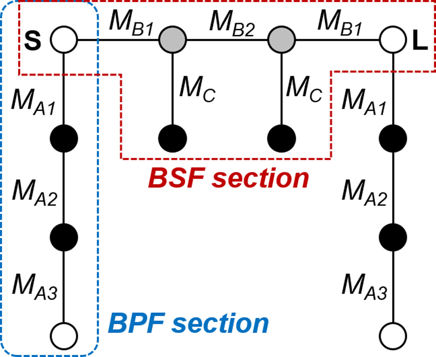
Fig. 8. Coupling-routing diagram of a second-order quasi-reflectionless BSF. White circles: source (S), load (L), and BPF-terminating resistors with resistance equal to the system impedance (Z0), gray circles: non-resonating nodes, black circles: resonating nodes, and connecting lines: couplings.

Fig. 9. Theoretically synthesized power transmission (|S21| = |S12|) and reflection (|S11| = |S22|) responses for single-stage, first- (Fig. 5), and second-order (Fig. 8) quasi-reflectionless BSFs. N = 1: M A = M C = 1.3, and M B = 1. N = 2: M A1 = 1.07, M A2 = 1.24, M A3 = 1.16, M B1 = 0.55, M B2 = 0.3, and M C = 0.85.
Quasi-reflectionless multi-band filters
In addition to the realization of single-band BPFs and BSFs with quasi-reflectionless capabilities, the proposed filter concept can be extended to multi-band BPF and BSF transfer functions. This can be achieved by expanding the resonating nodes in the single-band designs to multi-resonant ones, each of which controls the location of each band. As an example, Fig. 10 shows the coupling-routing diagram of a quasi-reflectionless first-order dual-band BPF. The dual-band behavior is obtained as follows. The resonator of the BPF section in Fig. 1 has been expanded to a dual-band resonant structure shaped by two resonating nodes (R 1 and R 2), three impedance inverters (α 1, α 2, and M D) and two non-resonating nodes. R 1 and R 2 respectively resonate at f 1 and f 2 and set the center frequency of each band and α 1 and α 2 control the BW of each band which can be designed independently. In order to obtain a quasi-reflectionless behavior in both bands, the BSF sections need to also have multi-resonant sections that are shaped by two resonating nodes R 1 and R 2 that respectively resonate at f 1 and f 2, two impedance inverters (M C1 and M C2) and one non-resonating node. In addition, the coupling coefficients must satisfy the following condition: M Cx = α x × M A × M B where x = 1, 2. Multiple ideally synthesized power transmission and reflection responses are shown in Fig. 11 in order to demonstrate the design principles of the quasi-reflectionless dual-band BPF in Fig. 10. As it can be seen, the BWs of the two passbands can be set to be equal or unequal. This is done in these examples by modifying the coupling coefficient α 1 that determines the BW of the lower passband. In a similar fashion, although not shown, the coefficient α 2 controls the BW of the upper passband.

Fig. 10. Coupling-routing diagram of a dual-band quasi-reflectionless BPF. White circles: source (S), load (L), and BSF-terminating resistors with resistance equal to the system impedance (Z0), gray circles: non-resonating nodes, black circles: resonating nodes, and connecting lines: couplings.
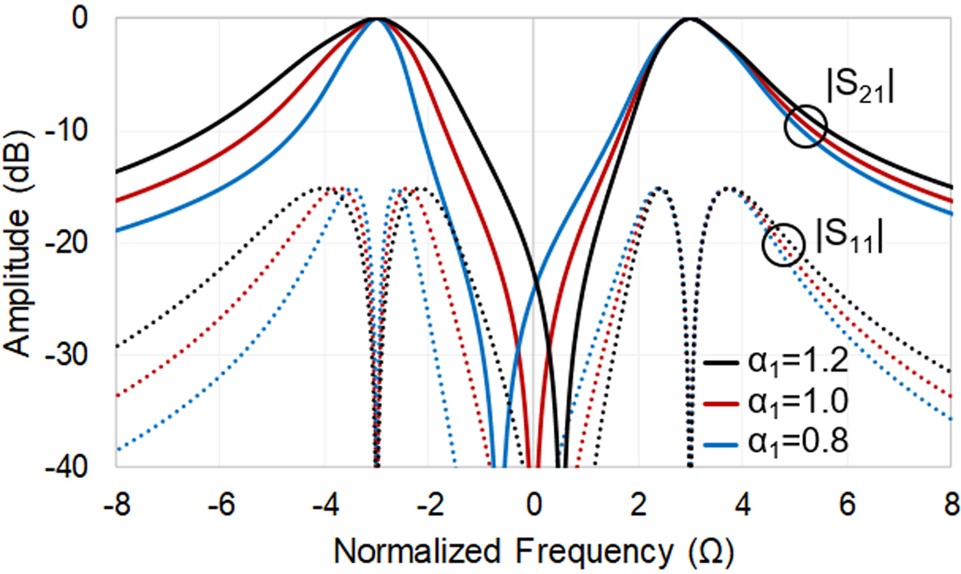
Fig. 11. Theoretically synthesized power transmission (|S21| = |S12|) and reflection (|S11| = |S22|) responses of a dual-band quasi-reflectionless BPF (Fig. 10) for alternative values of α 1 that result in passbands with different FBWs. For all responses: M A = M B = M C2 = M D = α 2 = 1, and M C1 = α 1MAMB.
Figure 12 shows the coupling-routing diagram of a quasi-reflectionless dual-band BSF. It was created by interchanging the dual-band BPF and BSF sections of the coupling-routing diagram in Fig. 10. In this manner, the power that is not transmitted from the source to the load through the BSF in its dual stopbands is absorbed in the resistors that are added at the ends of the BPF sections. Similar to the dual-band BPF design, R 1 and R 2 resonate at the frequencies f 1 and f 2 of the two desired stopbands and the following equation must be satisfied: M Cx = α x×M A×M B where x = 1, 2. To verify that the coupling-routing diagram in Fig. 12 results in a quasi-reflectionless dual-band BSF design, various ideally synthesized responses are shown in Fig. 13. As it can be seen, the quasi-reflectionless behavior is obtained throughout the entire normalized frequency range. Furthermore, the coupling coefficient α 2 controls the BW of the upper stopband in these examples, with higher values resulting in wider BWs. It should be noted that, although not illustrated in these examples, the coefficient α 1 allows to control the BW of the lower stopband in the same fashion.

Fig. 12. Coupling-routing diagram of a dual-band quasi-reflectionless BSF. White circles: source (S), load (L), and BPF-terminating resistors with resistance equal to the system impedance (Z0), gray circles: non-resonating nodes, black circles: resonating nodes, and connecting lines: couplings.

Fig. 13. Theoretically synthesized power transmission (|S21| = |S12|) and reflection (|S11| = |S22|) responses for a quasi-reflectionless dual-band BSF (Fig. 12) for different values of α 2 that result in stopbands with different FBWs. For all responses: M A = M C1 = 0.6, M B = M D = α 1 = 1, and M C2 = α 2MAMB.
Experimental results
In order to experimentally validate the proposed quasi-reflectionless filter concepts, three prototypes–one- and two-stage BPFs and a second-order BSF, respectively–were designed, manufactured, and measured. The two BPF prototypes were designed at a center frequency of 2 GHz and were built on a Rogers RO4003C substrate with the following characteristics: relative permittivity ε r = 3.38, thickness H = 1.52 mm, and dielectric loss tangent tanδ D = 0.0021. The BSF prototype was designed at a center frequency of 1 GHz and was built on a Rogers RO4350B substrate with the following characteristics: ε r = 3.48, H = 1.52 mm, and tanδ D = 0.0037. All three designs were carried out using the RF design principles in the section ‘Theoretical background’ for their theoretical synthesis and the software package Advanced Design System (ADS) from Keysight Technologies for their simulation and optimization. Their RF performances were experimentally validated with a Keysight N5224A PNA in terms of S-parameters.
One-stage bandpass filter
The layout and a photograph of the manufactured single-stage quasi-reflectionless BPF are shown in Figs 14(a) and 14(b), respectively. For size compactness, a mixed-technology integration scheme has been followed. In particular, the BPF sections were realized through microstrip-type half-wavelength (at 2 GHz) resonators and quarter-wavelength (at 2 GHz) transmission line-based impedance inverters. The BSF sections were materialized by means of series-type lumped-element resonators and lumped-element impedance inverters. In order to reduce the number of components, the parallel resonators were transformed to series through M C and, as such, the impedance inverter M C can be eliminated. Similarly, the impedance inverter M B can be excluded by transforming the termination resistors Z0 to M B2/Z0. A comparison of the RF-measured and EM-simulated power transmission and reflection responses and the group-delay curves for this prototype is provided in Fig. 15. The obtained agreement between simulated and measured results successfully validates the proposed quasi-reflectionless BPF concept. Its main measured RF performance metrics can be summarized as follows: center frequency of 2.04 GHz, 3-dB-referred BW of 184 MHz (i.e., of 9% in relative terms), minimum in-band IL of 1.49 dB, passband in-band group delay variation between 0.4 and 2.3 ns, and RL levels greater than 14.5 dB throughout the passband and larger than 10 dB in the range 1.04–3.43 GHz (i.e., 3.3:1 ratio). This corresponds to a quasi-reflectionless FBW of 117%.
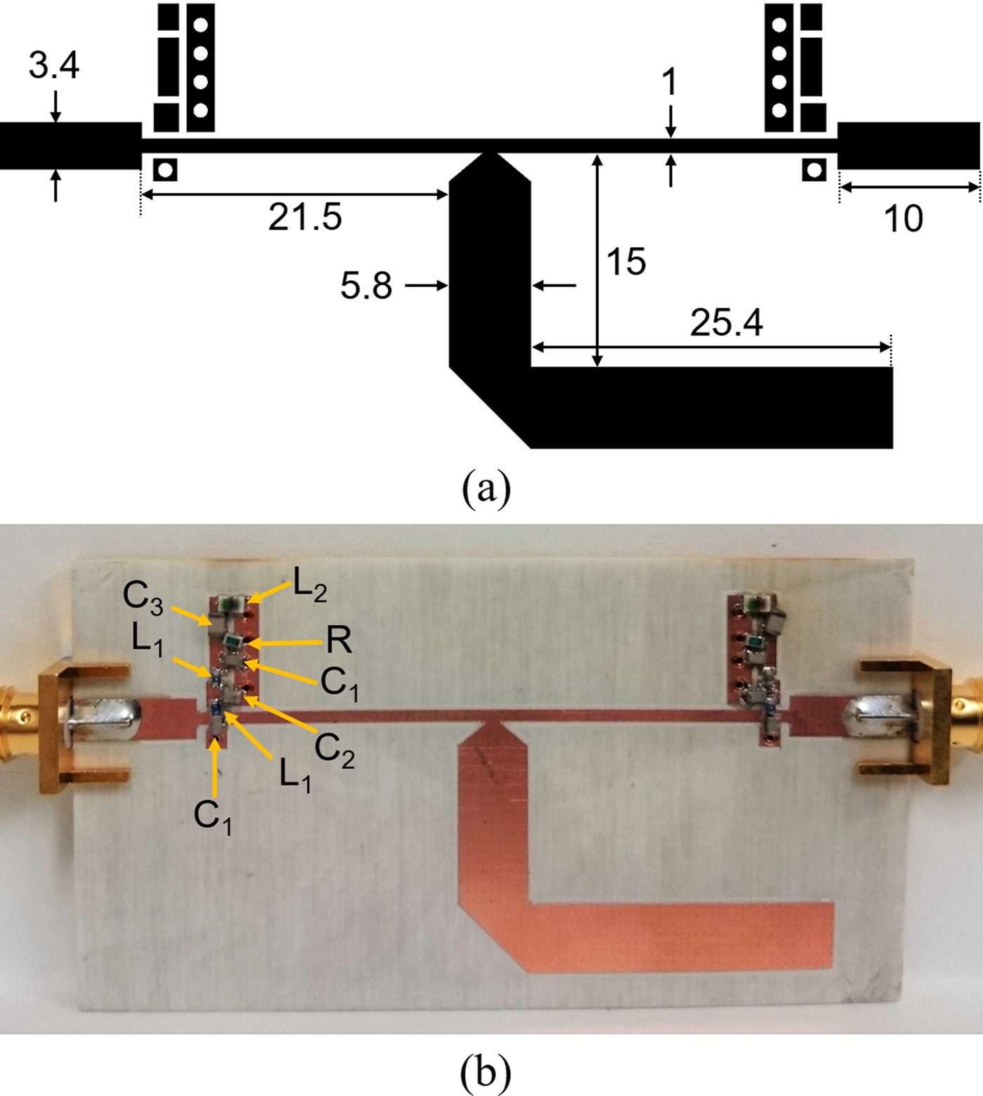
Fig. 14. (a) Layout of the single-stage quasi-reflectionless BPF (dimensions in mm). (b) Photograph of the manufactured prototype. Overall dimensions: 68.8 × 37.3 mm2. R = 46 Ω. All inductors are from Coilcraft: L 1 = 2.4 nH (0402HP-2N4) and L 2 = 10 nH (0805HT-10N). All capacitors are from Johanson Technology: C 1 = 0.3 pF (251R14S0R3BV4S), C 2 = 1.0 pF (251R14S1R0BV4S), and C 3 = 0.3 pF (251R15S0R3BV4S).

Fig. 15. RF-measured and EM-simulated responses of the single-stage quasi-reflectionless BPF in Fig. 14. (a) Power transmission (|S21|) and reflection (|S11|) responses. (b) Detail of the group-delay response.
Two-stage bandpass filter
The second prototype that was manufactured for validation purposes is a two-stage quasi-reflectionless BPF that is based on the design method in the section ‘Theoretical background’. Its layout and a photograph are presented in Figs 16(a) and 16(b), respectively. The RF-measured and EM-simulated power transmission and reflection responses and the group-delay curve of this circuit are compared in Fig. 17, showing again a fairly-close agreement. Its main measured RF performance characteristics are as follows: center frequency of 2.01 GHz, 3-dB-referred BW of 140 MHz (i.e., of 7% in relative terms), minimum in-band IL of 2.78 dB, passband group delay variation between 1 and 3.9 ns, and RL levels greater than 14.4 dB throughout the passband and over 10 dB in the range 1.13–3.37 GHz (i.e., 3:1 ratio). This corresponds to a quasi-reflectionless FBW of 111%.
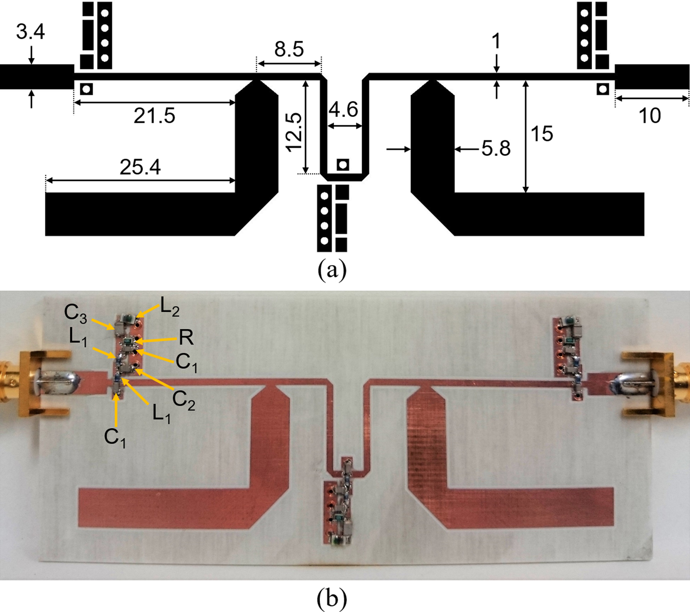
Fig. 16. (a) Layout of the two-stage quasi-reflectionless BPF (dimensions in mm). (b) Photograph of the manufactured prototype. Overall dimensions: 92.4 × 39.5 mm2. R = 46 Ω. All inductors are from Coilcraft: L 1 = 2.4 nH (0402HP-2N4) and L 2 = 10 nH (0805HT-10N). All capacitors are from Johanson Technology: C 1 = 0.3 pF (251R14S0R3BV4S), C 2 = 1.0 pF (251R14S1R0BV4S), and C 3 = 0.3 pF (251R15S0R3BV4S).

Fig. 17. RF-measured and EM-simulated responses of the two-stage quasi-reflectionless BPF in Fig. 16. (a) Power transmission (|S21|) and reflection (|S11|) responses. (b) Detail of the group-delay response.
Second-order bandstop filter
In order to validate the multi-order quasi-reflectionless filter concept, a second-order BSF was designed, manufactured, and measured. The layout and a photograph of the developed second-order quasi-reflectionless BSF prototype are presented in Figs 18(a) and 18(b), respectively. The second-order BSF section was implemented with quarter-wavelength (at 1 GHz) transmission-line impedance inverters and short-circuited quarter-wavelength-long (at 1 GHz) resonators. The resistively-terminated second-order BPF sections were realized using lumped-element impedance inverters (lowpass pi-type) and parallel-type resonators. The impedance inverter M A3 was excluded by transforming the system-impedance resistor Z0 to M A32/Z0. The RF-measured and EM-simulated power transmission and reflection responses and group-delay curves are compared in Fig. 19. The measured center frequency and 3-dB-referred BW are 990 MHz and 126 MHz (i.e., 12.7%), respectively. The prototype exhibits a minimum passband IL of 0.24 dB and maximum stopband rejection of 49.5 dB. Furthermore, the RL levels are greater than 15 dB within the stopband region and greater than 10 dB in the range 0.49–1.47 GHz (i.e., 3:1 ratio), which corresponds to a quasi-reflectionless FBW of 99%. Note also that the passband range of this second-order BSF is limited to the range 0.43–1.55 GHz due to the frequency dependence of the impedance inverters that is not contemplated by the coupling-routing diagram formalism.

Fig. 18. (a) Layout of the second-order quasi-reflectionless BSF (dimensions in mm). (b) Photograph of the manufactured prototype. Overall dimensions: 31 × 139 mm2. R = 133 Ω. All the inductors are from Coilcraft: L 1 = 12 nH (0806SQ-12N), L 2 = 2.6 nH (0604HQ-2N6), L 3 = 19 nH (0806SQ-19N), and L 4 = 2.1 nH (0403HQ-2N1). All capacitors are from Johanson Technology: C 1 = 1.5 pF (251R15S1R5BV4S), C 2 = 8.2 pF (251R15S8R2CV4S), and C 3 = 9.1 pF (251R15S9R1CV4S).

Fig. 19. RF-measured and EM-simulated responses of the second-order quasi-reflectionless BSF in Fig. 18. (a) Power transmission (|S21|) and reflection (|S11|) responses. (b) Detail of the group-delay response.
Comparison with state-of-the-art
Table 1 compares the RF-measured performance metrics of the developed quasi-reflectionless filter prototypes and some relevant state-of-the-art (SOA) reflectionless filters. As it can be seen, the proposed mixed-technology lumped-element/microstrip implementation approach that is used in this work results in performance and size advantages in comparison to SOA. Specifically, the proposed filters operate at higher frequencies and have lower minimum IL levels in the passband ranges than filter designs that only use lumped elements (e.g., 0.24 dB in the proposed BSF as oppose to 0.59 dB in the BSF in [Reference Lee, Kim, Lee, Chappell and Lee3] and 1 dB in the BSFs in [Reference Chieh and Rowland4, Reference Chieh and Rowland5]). Furthermore, they are smaller in area than filters that utilize only microstrip/distributed elements (e.g., the ones in [Reference Chieh and Rowland4–Reference Guyette, Hunter and Pollard6] and [Reference Psychogiou and Gómez-García9]). In addition to the aforementioned merits, the proposed quasi-reflectionless RF filters exhibit the widest reflectionless BW in which |S11|< −10 dB. Moreover, the proposed concepts can be readily extended to the realization of multi-band BPF and BSF transfer functions which are reported in this work for the first time. It should be noted that none of the filters that are summarized in Table 1 exhibits multi-band BPF or BSF response.
Table 1. Comparison of reflectionless filters.

λo, free space wavelength at f cen; LE, lumped element; M, microstrip; N/A, not applicable.
Conclusion
A new class of quasi-reflectionless BPFs, BSFs, and multi-band filters has been presented. The proposed filter concepts are based on conventional RF filtering sections that set the desired power transmission response and are loaded at their input/output ports with two auxiliary resistively-terminated frequency-selective filter sections. In order to obtain a quasi-reflectionless behavior, the auxiliary RF filtering sections need to exhibit complementary transfer functions with regard to the main one. In this manner, any RF signal that is not transmitted from the input to the output in the filter stopband regions is absorbed by the resistors. The theoretical foundations were first presented through a first-order single-stage BPF. Then, this approach was extended to multi-stage BPFs, multi-stage and higher-order BSFs, and multi-band BPFs and BSFs. For size compactness, a mixed-technology scheme, in which the main filter section can be realized with high-Q microstrip elements and the resistively-terminated auxiliary sections with lower-Q lumped-elements, was implemented. This design method leads to almost no size increase in relation to distributed reflective type filters. Three prototypes were manufactured and measured to experimentally validate the proposed coupling-routing diagrams. They include one- and two-stage BPFs designed at 2 GHz and a second-order BSF designed at 1 GHz. Their measured performances show that they retain a quasi- reflectionless behavior throughout a 99% FBW or greater, hence validating the presented design methodology.
Author ORCIDs
Dakotah J. Simpson, 0000-0002-7821-9884.
Acknowledgements
This work has been supported in part by the National Science Foundation, award number 1731956, the IEEE MTT-S Graduate Fellowship, and by the Spanish Ministry of Economy and Competitiveness under Project TEC2017-82398-R. The authors would like to thank Keysight for providing access to the software package ADS.
 Dakotah J. Simpson was born in Thornton, CO, USA in 1994. He received the B.S. degree in Electrical Engineering from the South Dakota School of Mines and Technology, Rapid City, South Dakota, in 2017. He is currently pursuing the Ph.D. degree in Electrical Engineering at the University of Colorado at Boulder, CO, USA. His current research interests include the design, characterization, and synthesis of reconfigurable microwave single-ended and balanced filters. Mr. Simpson is a member of the IEEE Microwave Theory and Techniques Society (IEEE MTT-S) and the Applied Computational Electromagnetics Society (ACES). He is the recipient of the MTT-S 2018 Graduate Fellowship, the University of Colorado's Dean's Graduate Assistantship and the ECEE Gold Award for Research.
 Roberto Gómez-García was born in Madrid, Spain, in 1977. He received the Telecommunication Engineering and Ph.D. degrees from the Polytechnic University of Madrid, Madrid, Spain, in 2001 and 2006, respectively. Since 2006, he has been an Associate Professor with the Department of Signal Theory and Communications, University of Alcalá, Alcalá de Henares, Spain. He has had several research stays with the C2S2 Department, XLIM Research Institute (formerly IRCOM), University of Limoges, Limoges, France; Telecommunications Institute, University of Aveiro, Aveiro, Portugal; US Naval Research Laboratory, Microwave Technology Branch, Washington, DC, USA; and Purdue University, West Lafayette, IN, USA. He is currently an Adjunct Part-Time Professor with the University of Electronic Science and Technology of China, Chengdu, China. His current research interests include the design of fixed/tunable high-frequency filters and multiplexers in planar, hybrid and MMIC technologies, multifunction circuits and systems, and software-defined radio and radar architectures for telecommunications, and remote sensing and biomedical applications.
 Dimitra Psychogiou received the Dipl.-Eng. degree in Electrical and Computer Engineering from the University of Patras, Patras, Greece, in 2008, and the Ph.D. degree in Electrical Engineering from the Swiss Federal Institute of Technology, Zürich, Switzerland, in 2013. From 2013 to 2016, she was a Post-Doctoral Research Associate and a Senior Research Scientist with Purdue University, West Lafayette, IN, USA. She is currently an Assistant Professor of Electrical, Computer and Energy Engineering with the University of Colorado at Boulder, Boulder, CO, USA. Her current research interests include the RF design and characterization of reconfigurable microwave and millimeter-wave passive components, RF-MEMS, acoustic-wave-resonator based filters, tunable filter synthesis, and frequency-agile antennas.


