


Introduction
With the development of miniaturization of the present device, decoupling becomes an essential concern in multiple antenna systems, such as in phased array and multi-input-multi-output antennas. Two techniques are generally used for decoupling between patch antennas: (a) change the patch position or shape it and (b) keep the original structure and add a decoupling structure between the patches. In [Reference Zhang, Ye, Frølund Pedersen and Zhang1], the patches are placed along the diagonal direction to reduce the coupling. In [Reference Chung and Kharkovsky2], the patches are rotated along the diagonal. In [Reference Liu, Zhu, Liu, Li, Fu and Liu3], two orthogonal slots on the two adjacent patches were cut along the diagonal and combined with shorting pin to reduce the mutual coupling. However, the most common decoupling technique is the second technique of keeping the original structure and inserting a decoupling structure.
Much work has been presented for decoupling patch antennas where the shape and placement are used. Furthermore, adding a loading structure on top of the patches was used [Reference Li, Zhong and Cheung4–Reference Li, Jiang and Yeung6]. Also, adding a planar structure between the patches was employed [Reference Alsath, Kanagasabai and Balasubramanian7, Reference Yang, Liu, Xu and Gong8] as an effective decoupling method. Except these, no additional decoupling techniques were proposed where the weak current distributions are analyzed [Reference Lin, Chen, Ji, Yang, Wang and Ge9, Reference Lai, Pan, Zheng and Yang10].
However, it was noticed that interference with the decoupling structure causes a tilt for the embedded radiation pattern. This phenomenon exists when a large edge-to-edge distance of over 0.125λ 0 [Reference Yang, Peng, Liao, Mo, Jiang and Li11–Reference Yang, Liu, Zhou and Cui15] exists, where λ 0 is the free space wavelength. Edge-to-edge distance of 0.3λ 0 and 0.25λ 0 in [Reference Yang, Peng, Liao, Mo, Jiang and Li11] and [Reference Bait-Suwailam, Siddiqui and Ramahi12], respectively, had tilted the peak by 10° and 20° at 4.6 GHz. In [Reference Wei, Li, Wang, Xing and Xu13–Reference Yang, Liu, Zhou and Cui15], the tilt angles were over 10° for distances around 0.13λ 0. As edges get closer to each other, the mutual coupling gets stronger, and the present decoupling techniques for the closer distances of about 0.05λ 0 show a pattern peak tilt characteristic [Reference Sun and Cao16–Reference Qi, Liu, Yin, Zhao and Kulesza23]. For a distance greater than 0.05λ 0, the tilt was over 15° [Reference Sun and Cao16–Reference Gao, Cao, Fu, Quan and Chen20]. The tilt depends on the adopted decoupling methods, which means the tilt angle will not increase as the distance decreases, as the tilt angle was 20° when the distance was 0.077λ 0 [Reference Sun and Cao16], while it was 15° with 0.059λ 0 distance [Reference Dadashzadeh, Dadgarpour, Jolani and Virdee17]. A tilt of 30° for a distance of 0.06λ g [Reference Hwangbo, Yang and Yoon18], 0.07λ 0 [Reference Lu, Zhang, Qi, Li, Zhao and Yin19], and 0.057λ 0 [Reference Gao, Cao, Fu, Quan and Chen20] was reported, where λ g is the guided wavelength. A similar property was suited for the separations of less than 0.05λ 0 [Reference Habashi, Nourinia and Ghobadi21–Reference Qi, Liu, Yin, Zhao and Kulesza23]. In [Reference Habashi, Nourinia and Ghobadi21], the tilt is over 20° for 0.039λ 0 and over 35° for 0.031λ 0 [Reference OuYang, Yang and Wang22] but reduces to about 30° for 0.03λ 0 [Reference Qi, Liu, Yin, Zhao and Kulesza23].
Therefore, this study focuses on decoupling techniques with beam tilt correction for edge-to-edge distance of λ 0/20 along the H-plane. We used a 3D vertical wall to realize a single frequency pattern correction [Reference Wang, Zhang, Yan, Yu and Kishk24] and a realized gain increase using a lower-loss substrate [Reference Wang, Zhang, Wang, Lan, Yu, Mo and Kishk25]. The present paper proposes a decoupling structure for a beam tilt correction within the whole operating frequency band of interest and a gain reduction of 0.6 dB compared to the no-decoupling case. Here, a 3D vertical wall of FR4 substrate with two-sided cladding is employed, and symmetrical slots on both sides are itched. The vertical conducting walls are connected to the horizontal ground plane of the patch antenna to form a resonant structure and induce reverse current on the wall to reduce the impact of the current generated by the patch. Consequently, the H-plane radiation patterns in the 5.80 GHz band are corrected.
The rest of the paper is organized as follows. The section “The proposed patch antennas” introduces the whole antenna configuration, including the details of the decoupling wall and the comparisons between the simulations and measurements for verification. Then, the tilt correction is analyzed by forming a resonator in the section “Result analysis.” The critical parameters are analyzed to explain their effects on tilt correction and decoupling. The current distributions are compared before and after decoupling. The final section is the conclusion.
The proposed patch antennas
An H-plane arranged two-patch antennas with an edge-to-edge distance of λ 0/20 is investigated. Then, the 3D metal-slotted vertical wall is inserted between the two patches to reduce the mutual coupling significantly. The details of the proposed technique and the optimized final antenna performance are as follows.
The antennas and decoupling structure
The antennas’ detailed configuration with the proposed 3D vertical wall is shown in Fig. 1, where the gray and gold colors represent the dielectric substrate and metal, respectively. The corresponding parameters of the patch antennas and the vertical wall are inserted. Figure 1(a) and (b) show top and side views of the structure, where the negative and the positive indicate the tilt directions from the broadside. The wall is embedded in the substrate and connected to the ground plane. Figure 1(c) indicates that the decoupling structure has three layers, the middle substrate layer and two symmetrical slotted metals. Figure 1(d) shows that the slot is symmetrically etched about the y-axis or the metal. The metal has a proper resonance length to introduce the reverse current from the ground plane, reducing the influence of the current induced on the wall from patch radiation

Figure 1. The patches and proposed decoupling structure: (a) top view, (b) side view, (c) exploded view of the vertical wall, and (d) side view of the vertical wall.
For the patch antenna design, the substrate F4BTM440 is utilized with a relative dielectric constant of 4.4 and a loss tangent of 0.0033. The conventional patch antenna with a length and width of 46 mm and 31.7 mm, respectively, are used to resonate at 5.80 GHz. Moreover, the quarter-wavelength impedance transformer is applied for impedance matching. Then, another similar patch antenna is placed parallel to the original one along the H-plane, where the edge-to-edge distance is 2.58 mm (about λ 0/20). After that, the proposed 3D vertical wall is inserted between the patches. Here, the FR4 material is taken as the substrate of the decoupling structure. Its higher dielectric loss will increase the loss of the wall. The relative dielectric constant and loss tangent of the FR4 are 4.4 and 0.025, respectively, and the thickness is 0.8 mm.
Antenna performance
After parametric analysis, we get the final optimized design parameters and results based on the abovementioned method. The corresponding values for the mentioned parameters are listed in Table 1. Photos of the fabricated prototype are shown in Fig. 2. The antenna is measured in the anechoic chamber, as shown in Fig. 3.
Table 1. Values of antenna parameters

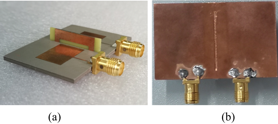
Figure 2. Antenna prototype: (a) 3D view and (b) back view.
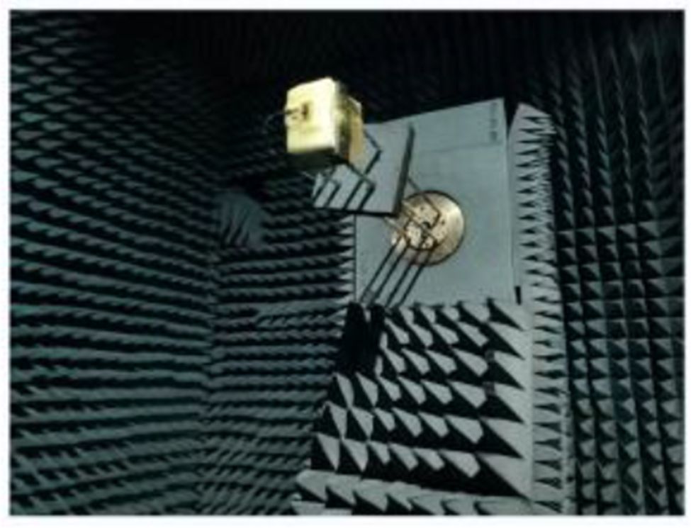
Figure 3. Measurement in an anechoic chamber.
The comparisons of the measured and simulated S-parameters are shown in Fig. 4(a). The comparisons show that the measurements agree well with the simulations, though a slight shift of the resonant frequency exists, and the measured S 21 is lower than that of the simulation. Here, the measured resonant frequency shifts by 50 MHz to 5.85 GHz, and the measured impedance bandwidth is 140 MHz from 5.78 to 5.92 GHz, which is 10 MHz less than the simulation. After adding the proposed structure, the isolation becomes better than that without a decoupling structure by 20 dB, which we can judge from the corresponding data of Fig. 4(a), where the measured S 21 are all below −30 dB in the entire bandwidth while they are over −10 dB of no-decoupling structure. The S-parameter comparisons of the no-decoupling structure and the complete wall are shown in Fig. 4(b), which indicates that the complete wall can improve the matching and the isolation if the wall’s dimension is proper.

Figure 4. S-parameters: (a) with and without decoupling structure and (b) no-decoupling vs. complete wall comparison.
The comparisons of radiation patterns, realized gains, and tilt angles between the simulations and measurements are shown in Figs. 5–7, respectively, where the left antenna of Fig. 1(a) is excited, and the patterns of no-decoupling structure and the complete vertical wall structure are depicted to be compared in Fig. 5. These three comparisons of the proposed structure indicate that the measurements agree well with those of simulations. We only present H-plane patterns because the decoupling arrangement has an insignificant effect on the E-plane patterns.

Figure 5. Normalized radiation pattern with and without decoupling structures at the simulated and measured resonance frequencies: (a) H-plane and (b) E-plane.
Figure 5 compares radiation patterns in the E- and H-plane with and without decoupling structure. Each case has a different resonant frequency. The no-decoupling case is considered at 5.78 GHz (simulated) and 5.85 GHz (measured). The proposed decoupling case is presented at 5.80 GHz (simulated) and 5.85 GHz (measured) by black and red lines, respectively. In contrast, the corresponding blue and green lines indicate simulated results of no-decoupling (no wall) and complete wall structures. The H-plane pattern peak direction of the no-decoupling structure is 27°, while it tilts to the other side, −19.5°, when the complete wall is employed, which is corrected to near the broadside direction after using the proposed structure.
The simulated bandwidth of the proposed structure shifts to a higher band due to the vertical wall, and the measured bandwidth also shifts slightly to a higher level than the simulation. Thus, we show the realized gain of the H-plane in their bandwidth in Fig. 6, where the frequency step is 0.01 GHz. After adding the decoupling structure, the simulated realized gain decreases, and the maximum difference is 0.86 dB. On the contrary, the measured realized gain is higher than the simulation for the proposed structure, but the maximum values appear near the corresponding resonances 5.79 GHz of simulation and 5.88 GHz of measurement, whose difference is 0.25 dB. This difference is because of fabrication error, in which we cannot ensure that the wall is grounded entirely. In addition, the measured result is closer to that with no-decoupling structure with a maximum difference of 0.6 dB.
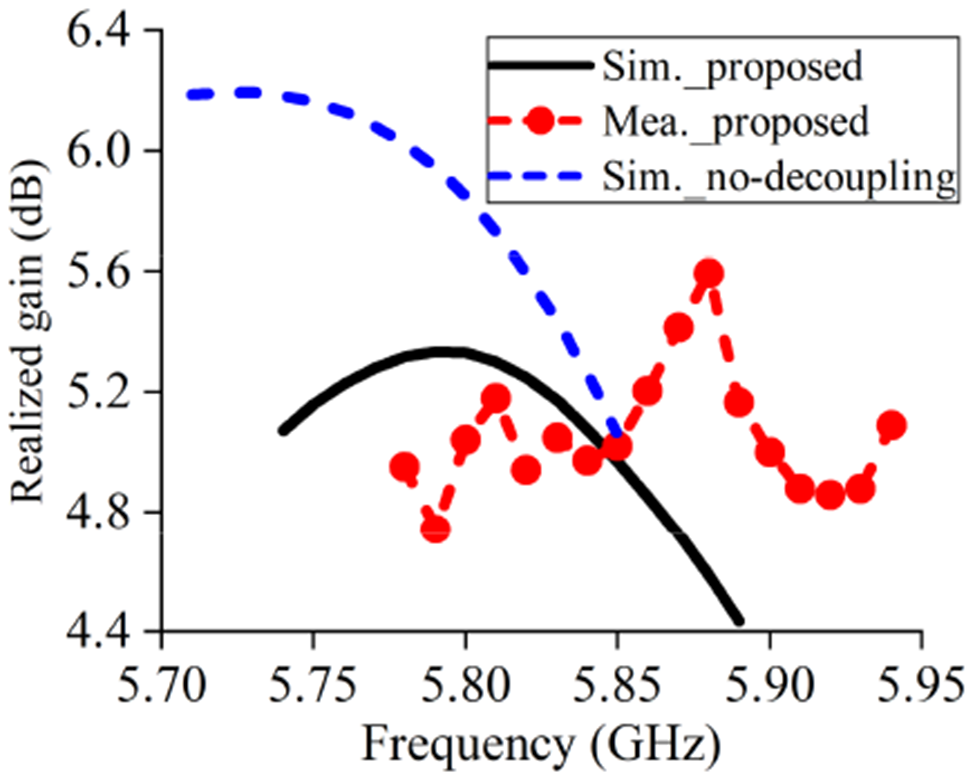
Figure 6. Realized gain comparisons in the bandwidth.
The tilt angles in the H-plane without decoupling structure are depicted in Fig. 7(a). In the simulated results, the tilts range from 22.5° to 28.5° in the bandwidth with frequency steps of 0.01 GHz. The tilts shown in Fig. 7(b) are reduced to be −6° to 3° range within 5.74 to 5.89 GHz, while the measured show the peak variation within −4.5° to 3° for the bandwidth of 5.78 to 5.92 GHz.

Figure 7. Tilt angle comparisons of H-plane in the bandwidth: (a) without decoupling and (b) with the proposed decoupling structure.
Result analysis
This section analyzes the proposed decoupling structure with the tilt correction by introducing the resonant dimension that induces a correction current on the wall. Then the influences of the main parameters are investigated, and finally, the decoupling effect is presented by the surface current on the patch antenna.
Tilt correction
As we know, the complete metal wall will play the role of decoupling because it can prevent the direct interference of the excited patch to another. However, the corresponding induced current on the wall affects the radiation performance, the matching, and the realized gain. Thus, we must design the complete wall carefully to get a good matching with the reduction of isolation. Figure 4(b) shows S-parameter comparisons of the no-decoupling case with the complete wall decoupling structure. The matching and the isolation are improved after carefully designing the complete wall, while the corresponding H-plane pattern, as shown in Fig. 5(a), tilts in the opposite direction. Because the most concerning problem in this study is the beam direction tilt, we have to modify the wall structure to make the induced current on the wall correct the beam direction rather than deteriorating it. It is found that connecting the wall to the ground, as shown in Fig. 1(b), helps make such a correction.
Exciting the patch antenna induces a current on a fixed area of the complete wall, whether the wall is grounded or not. Figure 8(a) indicates the current distribution for the complete grounded wall case and Fig. 8(b) for the case of the wall shifted up 0.1 mm (ungrounded). The current distributions in both cases are concentrated very close to the ground plane and mainly parallel to it. Thus, this current has an image in the opposite direction, making its broadside contribution very weak and insufficient to correct the beam tilt. A slot is introduced where the current is concentrated to remove the induced current close to the ground. Figure 8(c) shows the current distribution with the slot and grounded ends of the wall. It can be seen that introducing the slot shifts the induced strong current to the wall’s outer edges. The top edge, which is further away from the ground plane, acts close to a dipole parallel to the ground and a quarter wavelength from the ground (here, H s is about λ 0/8, but because of the dielectric of the substrate and the vertical wall dielectric, it seems that the equivalent electrical length of H s is close of a quarter of a wavelength), which contributes to the broadside radiation. The side edges act as two out-of-phase monopoles without contributing to the broadside. Thus, the structure radiation is influenced by the slotted vertical wall correcting the beam tilt. If the slotted wall is not grounded, the current distribution concentrates at the upper slot edge, as shown in Fig. 8(d). This current is much closer to the ground plane. Thus, its image current is the opposite, making a feeble contribution to the broadside direction. Thus, the beam tilt is not corrected.

Figure 8. Current distribution comparisons on the vertical wall, (a) grounded whole wall, (b) ungrounded wall, (c) slot in the middle of the wall with grounded ends, and (d) slot with ungrounded ends of the wall.
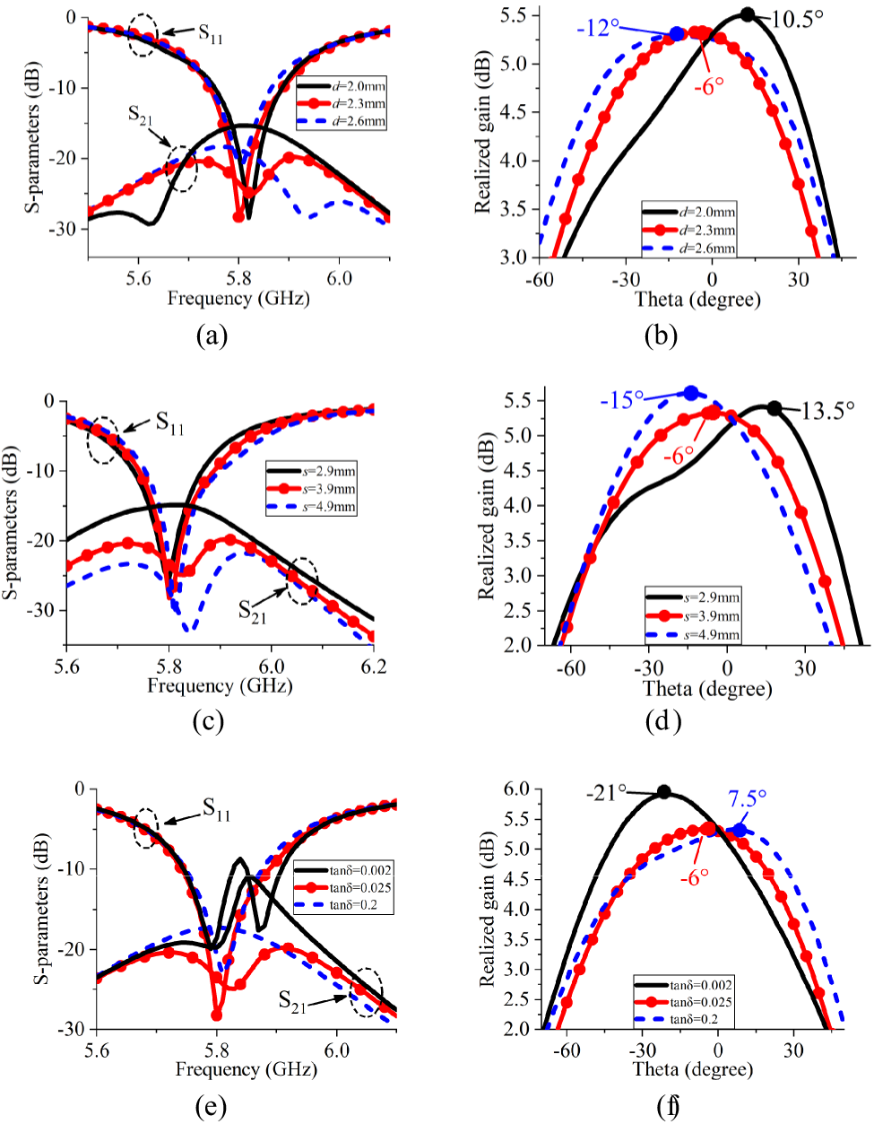
Figure 9. Parameter analysis: (a) S-parameter with d, (b) H-plane realized gain at 5.8 GHz with d, (c) S-parameter with s, (d) H-plane realized gain at 5.8 GHz with s, (e) S-parameters with wall dielectric loss, and (f) 5.8 GHz realized gains of H-plane with wall dielectric loss.
Parameter analysis
All the variables of the vertical wall will affect the matching, decoupling, and pattern tilt of the H-plane. However, the influences of some variables are obvious, such as the height and the width of the wall. So, we pick up two main variables of dimensions d and s to analyze their influences while the size of the metal is fixed and change the loss tangent of the wall substrate to analyze its effect on the S-parameters and gain. The height of the protruding part of the wall that is H s − H 0 is 4.9 mm (about 0.21λ, λ is the effective wavelength of FR4), and the width L 4 is 24 mm, about 1.05λ. The total width of the metal on the wall p is 18.8 mm, about 0.82λ. The influences of dimension variables are shown in Fig. 9(a–d), which involve the S-parameters and the pattern correction. They almost do not affect the reflection coefficient, except that the variable d has little effect on the resonance frequency and matching, but both affect the decoupling in the bandwidth. These two variables control the size of the slot, which affects the decoupling, but s has a more significant effect. On the contrary, both variables impact the angle of the pattern significantly, that is because they determine the strength of the introduced current (d) or the induced current (s) on the wall. In other words, the final current of the middle part depends on the superposition of the two currents. Figure 9(e) and (f) shows the effect of loss tangent on the antenna performance. This variable affects not only the matching and isolation but also the tilt angle and the realized gain if the size is not changed. This indicates that we should define the corresponding structure parameters for one fixed loss tangent of the wall substrate.
Current distribution on patch
Figure 10 compares current distributions on the two patches at resonances before and after using the proposed structure. The antenna on the left is excited, and a matching load terminates the antenna on the right. The coupled current has been suppressed significantly.

Figure 10. Current distributions on patches at resonances (a) without and (b) with the proposed wall.
Conclusion
The main goal of the present work was to decrease the mutual coupling and correct the beam tilt usually caused by the coupling between the two tightly spaced patches in the H-plane. A vertical wall between the two patches was introduced, reducing the mutual coupling but not correcting the beam tilt. To correct the radiation beam, a slot was introduced on the wall close to the ground plane that perturbed the induced current to influence the radiation characteristics and correct the beam tilt. The proposed structure has been fabricated and measured. After carefully adjusting the corresponding wall parameters, the main beam direction was within the −4.5° to 3° from the broadside direction with a 0.60 dB reduction of the maximum realized gain compared to the simulated one without a decoupling structure. The measurements have agreed well with the simulations.
Financial support
This work was supported by the Natural Science Foundation of Guangxi Province (grant number 2019GXNSFFA245002); the National Natural Science Foundation of China (grant number 12161025 and 62071057); and the Guangxi Key Laboratory of Wireless Wideband Communication and Signal Processing (grant number GXKL06200123 and GXKL06230105).
Competing interests
The authors report no conflict of interest.


