Hostname: page-component-848d4c4894-2xdlg Total loading time: 0 Render date: 2024-07-06T18:25:42.608Z Has data issue: false hasContentIssue false

Focused electron beam-induced deposition at cryogenic temperatures

Published online by Cambridge University Press:  04 February 2011

M. Bresin
Affiliation:
College of Nanoscale Science and Engineering, University at Albany, Albany, New York 12203
B.L. Thiel
Affiliation:
College of Nanoscale Science and Engineering, University at Albany, Albany, New York 12203
M. Toth
Affiliation:
College of Nanoscale Science and Engineering, University at Albany, Albany, New York 12203 FEI Company, Hillsboro, Oregon 97124
K.A. Dunn*
Affiliation:
College of Nanoscale Science and Engineering, University at Albany, Albany, New York 12203
*
a)Address all correspondence to this author. e-mail: kdunn1@uamail.albany.edu
Get access

Abstract

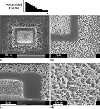
Direct-write, cryogenic electron beam-induced deposition (EBID) was performed by condensing methylcyclopentadienyl-platinum-trimethyl precursor onto a substrate at −155 °C, exposing the condensate by a 15 keV electron beam, and desorbing unexposed precursor molecules by heating the substrate to room temperature. Dependencies of film thickness, microstructure, and surface morphology on electron beam flux and fluence, and Monte Carlo simulations of electron interactions with the condensate are used to construct a model of cryogenic EBID that is contrasted to existing models of conventional, room temperature EBID. It is shown that material grown from a cryogenic condensate exhibits one of three distinct surface morphologies: a nanoporous mesh with a high surface-to-volume ratio; a smooth, continuous film analogous to material typically grown by room temperature EBID; or a film with a high degree of surface roughness, analogous to that of the cryogenic condensate. The surface morphology can be controlled reproducibly by the electron fluence used for exposure.

Type
Articles
Copyright
Copyright © Materials Research Society 2011

Access options

Get access to the full version of this content by using one of the access options below. (Log in options will check for institutional or personal access. Content may require purchase if you do not have access.)

References

REFERENCES

1.van Dorp, W.F. and Hagen, C.W.: A critical literature review of focused electron beam induced deposition. J. Appl. Phys. 104, 081301 (2008).CrossRefGoogle Scholar
2.Utke, I., Hoffman, P., and Melngailis, J.: Gas-assisted focused electron beam and ion beam processing and fabrication. J. Vac. Sci. Technol., B 26, 1197 (2008).CrossRefGoogle Scholar
3.Botman, A., Mulders, J.J.L., and Hagen, C.W.: Creating pure nanostructures from electron-beam-induced-deposition using purification techniques: A technology perspective. Nanotechnology 20, 372001 (2008).CrossRefGoogle Scholar
4.Randolph, S.J., Fowlkes, J.D., and Rack, P.D.: Focused, nanoscale electron-beam-induced deposition and etching. Crit. Rev. Solid State Mater. Sci. 31, 55 (2006).CrossRefGoogle Scholar
5.Botman, A., Mulders, J.J.L., Weemaes, R., and Mentink, S.: Purification of platinum and gold structures after electron-beam-induced-deposition. Nanotechnology 15, 3779 (2006).CrossRefGoogle Scholar
6.Mölhave, K., Madsen, D.N., Rasmussen, A.N., Carlsson, A., Appel, C.C., Brorson, M., Jacobson, C.J.H., and Boggild, P.: Solid gold nanostructures fabricated by electron beam deposition. Nano Lett. 3, 1499 (2003).CrossRefGoogle Scholar
7.Bell, D.A., Falconer, J.L., Zhiming, L., and McConica, C.M.: Electron beam-induced deposition of tungsten. J. Vac. Sci. Technol., B 12, 2976 (1994).CrossRefGoogle Scholar
8.Funsten, H.O., Boring, J.W., Johnson, R.E., and Brown, W.L.: Low-temperature beam-induced deposition of thin tin films. J. Appl. Phys. 71, 1475 (1992).CrossRefGoogle Scholar
9.Park, Y.K., Nagai, T., Takai, M., Lehrer, C., Frey, L., and Ryssel, H.: Comparison of beam-induced deposition using ion microprobe. Nucl. Instrum. Methods Phys. Res., Sect. B 148, 25 (1999).CrossRefGoogle Scholar
10.Gopal, V., Stach, E.A., Radmilovic, V.R., and Mowat, I.A.: Metal delocalization and surface decoration in direct-write nanolithography by electron beam induced deposition. Appl. Phys. Lett. 85, 49 (2004).CrossRefGoogle Scholar
11.Hovington, P., Drouin, D., and Gauvin, R.: CASINO: A new Monte Carlo code in C language for electron beam interactions–Part I: Description of the program. Scanning 19, 1 (1997).CrossRefGoogle Scholar
12.Utke, I., Friedli, V., Amorosi, S., Michler, J., and Hoffman, P.: Measurement and simulation of impinging precursor molecule distribution in focused particle beam deposition/etch systems. Microelectron. Eng. 83, 1499 (2006).CrossRefGoogle Scholar
13.Zaykova-Feldman, L. and Moore, T.M.: The total release method for FIB in situ TEM sample preparation. Microsc. Microanal. 11(suppl 2), 848 (2005).CrossRefGoogle Scholar
14.Toth, M. and Philips, M.R.: Monte Carlo modeling of cathodoluminescence generation using electron energy loss curves. Scanning 20, 425 (1998).CrossRefGoogle Scholar
15.Xue, Z., Strouse, M.J., Shuh, D.K., Knobler, C.B., Kaesz, H.D., Hicks, R.F., and Williams, R.S.: Characterization of (methylcyclopentadienyl)trimethylplatinum and low-temperature organometallic chemical vapor deposition of platinum metal. J. Am. Chem. Soc. 111, 8779 (1989).CrossRefGoogle Scholar
16.Wnuk, J.D., Gorham, J.M., Rosenberg, S.G., van Dorp, W.F., Madey, T.E., Hagen, C.W., and Fairbrother, D.H.: Electron-induced surface reactions of the organometallic precursor trimethyl (methylcyclopentadienyl) platinum (IV). J. Phys. Chem. C 113, 2487 (2009).CrossRefGoogle Scholar
17.JCPDS card 04-08025.Google Scholar
18.Frabboni, S., Gazzadi, G.C., and Spessot, A.: TEM study of the annealed Pt nanostructures grown by electron beam-induced deposition. Physica E 37, 265 (2007).CrossRefGoogle Scholar
19.Koops, H.W.P., Kaya, A., and Weber, M.: Fabrication and characterization of platinum nanocrystalline material grown by electron-beam induced deposition. J. Vac. Sci. Technol. B, 13, 2400 (1995).CrossRefGoogle Scholar
20.Botman, A., Hesselberth, M., and Mulders, J.J.L.: Improving the conductivity of platinum-containing nano-structures created by electron-beam-induced deposition. Microelectron. Eng. 85, 1139 (2008).CrossRefGoogle Scholar
21.Yavas, O., Ochiai, C., Takai, M., Hosono, A., and Okuda, S.: Maskless fabrication of field-emitter array by focused ion and electron beam. Appl. Phys. Lett. 76, 3319 (2000).CrossRefGoogle Scholar
22.van Dorp, W.F., Wnuk, J.D., Gorham, J.M., Fairbrother, D.H., Madey, T.E., and Hagen, C.W.: Electron induced dissociation of trimethyl (methylcyclopentadienyl) platinum (IV): Total cross section as a function of incident electron energy. J. Appl. Phys. 106, 074903 (2009).CrossRefGoogle Scholar
23.Botman, A., de Winter, D.A.M., and Mulders, J.J.L.: Electron-beam-induced deposition of platinum at low landing energies. J. Vac. Sci. Technol., B 26, 2460 (2008).CrossRefGoogle Scholar
24.Lobo, C.J., Toth, M., Wagner, R., Thiel, B.L., and Lysaght, M.: High resolution radially symmetric nanostructures from simultaneous electron beam induced etching and deposition. Nanotechnology 19, 025303 (2008).CrossRefGoogle ScholarPubMed
25.Smith, D.A., Fowlkes, J.D., and Rack, P.D.: A nanoscale three-dimensional Monte Carlo simulation of electron-beam-induced deposition with gas dynamics. Nanotechnology 18, 265308 (2007).CrossRefGoogle ScholarPubMed
26.Everhart, T.E. and Hoff, P.H.: Determination of kilovolt electron energy dissipation vs penetration distance in solid materials. J. Appl. Phys. 42, 5837 (1971).CrossRefGoogle Scholar
27.Goldstein, J.I., Newbury, D.E., Echlin, P., Joy, D.C., Roming, A.D. Jr., Lyman, C.E., Fiori, C., and Lifshin, E.: Scanning Electron Microscopy and X-ray Microanalysis, 2nd ed. (Plenum, New York, 1992).CrossRefGoogle Scholar
28.Li, J., Toth, M., Tileli, V., Dunn, K.A., Lobo, C.J., and Thiel, B.L.: Evolution of the nanostructure of deposits grown by electron beam induced deposition. Appl. Phys. Lett. 93, 023130 (2008).CrossRefGoogle Scholar
29.Botman, A., Hagen, C.W., Li, J., Thiel, B.L., Dunn, K.A., Mulders, J.J.L., Randolph, S., and Toth, M.: Electron post-irradiation of platinum-containing nanostructures grown by electron-beam-induced deposition from Pt(PF3)4. J. Vac. Sci. Technol., B 27, 2759 (2009).CrossRefGoogle Scholar
30.Li, J., Toth, M., Dunn, K.A., Moore, R.L., and Thiel, B.L.: Structure of Pt-containing nanocomposites grown by room temperature electron beam induced deposition. J. Appl. Phys. (in press).Google Scholar
31.Harriott, L.R., Cummings, K.D., Gross, M.E., and Brown, W.L.: Decomposition of palladium acetate films with a microfocused ion beam. Appl. Phys. Lett. 49, 1661 (1986).CrossRefGoogle Scholar
32.Hoffman, P., Ben Assayag, G., Gierak, J., Flicstein, J., Maar-Stumm, M., and van den Bergh, H.: Direct writing of gold nanostructures using a gold-cluster compound and a focused-ion beam. J. Appl. Phys. 74, 7588 (1993).CrossRefGoogle Scholar
33.Stark, T.J., Mayer, T.M., Griffis, D.P., and Russell, P.E.: Electron beam induced metallization of palladium acetate. J. Vac. Sci. Technol., B 9, 3475 (1991).CrossRefGoogle Scholar
34.Marqués-Hueso, J., Abargues, R., Canet-Ferrer, J., Agouram, S., Valdés, J.L., and Martinez-Pastor, J.P.: Au-PVA nanocomposite negative tone resist for one-step three-dimensional e-beam lithography. Langmuir 26, 2825 (2010).CrossRefGoogle ScholarPubMed
35.Abargues, R., Marqués-Hueso, J., Canet-Ferrer, J., Pedrueza, E., Valdés, J.L., Jiménez, E., and Martinez-Pastor, J.P.: High-resolution electron-beam patternable nanocomposite containing metal nanoparticles for plasmonics. Nanotechnology 19, 355308 (2008).CrossRefGoogle ScholarPubMed