Hostname: page-component-78c5997874-t5tsf Total loading time: 0 Render date: 2024-11-18T05:43:39.222Z Has data issue: false hasContentIssue false

Deposition and characterization of nanostructured Cu2O thin-film for potential photovoltaic applications

Published online by Cambridge University Press:  11 June 2013

Nishant Gupta
Affiliation:
Holcombe Department of Electrical and Computer Engineering, Clemson University, Clemson, South Carolina 29634
Rajendra Singh*
Affiliation:
Holcombe Department of Electrical and Computer Engineering, Clemson University, Clemson, South Carolina 29634
Fan Wu
Affiliation:
Department of Materials Science and Engineering, North Carolina State University, Raleigh, North Carolina 27695-7907
Jagdish Narayan
Affiliation:
Department of Materials Science and Engineering, North Carolina State University, Raleigh, North Carolina 27695-7907
Colin McMillen
Affiliation:
Department of Chemistry, Clemson University, Clemson, South Carolina 29634
Githin F. Alapatt
Affiliation:
Holcombe Department of Electrical and Computer Engineering, Clemson University, Clemson, South Carolina 29634
Kelvin F. Poole
Affiliation:
Holcombe Department of Electrical and Computer Engineering, Clemson University, Clemson, South Carolina 29634
Shiou-Jyh Hwu
Affiliation:
Department of Chemistry, Clemson University, Clemson, South Carolina 29634
Dino Sulejmanovic
Affiliation:
Department of Chemistry, Clemson University, Clemson, South Carolina 29634
Matthew Young
Affiliation:
National Renewable Energy Laboratory, Golden, Colorado 80401
Glenn Teeter
Affiliation:
National Renewable Energy Laboratory, Golden, Colorado 80401
Harin S. Ullal
Affiliation:
National Renewable Energy Laboratory, Golden, Colorado 80401
*
a)Address all correspondence to this author. e-mail: srajend@clemson.edu
Get access

Abstract

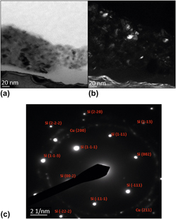
Copper (I) oxide (Cu2O) is a direct band gap semiconductor with p-type conductivity and is a potential candidate for multi-junction solar cells. In this work, incoherent light source based photo-assisted metal-organic chemical vapor deposition (MOCVD) was used to deposit high quality Cu2O thin films on n-type <100> silicon and quartz substrates. X-ray diffraction studies reveal that crystalline Cu2O is deposited. UV-Vis-NIR spectroscopy results indicated a band gap of 2.44 eV for Cu2O thin films. Transmission electron spectroscopy results show that the Cu2O film grows in the form of three-dimensional islands composed of smaller nanocrystalline grains in the range of 10–20 nm. IV measurements indicate that the Cu2O/n-Si device fabricated using the MOCVD process has a lower dark current density than other devices reported in the literature.

Type
Articles
Copyright
Copyright © Materials Research Society 2013 

Access options

Get access to the full version of this content by using one of the access options below. (Log in options will check for institutional or personal access. Content may require purchase if you do not have access.)

References

REFERENCES

Solar markets: Overall Growth & Size by Country, available: http://solarcellcentral.com/markets_page.html, June 2012.Google Scholar
Singh, R. and Leslie, J.D.: Economic requirements for new materials for solar photovoltaic cells. Sol. Energy 24(6), 589 (1980).CrossRefGoogle Scholar
Green, M.A.: The path to 25% silicon solar cell efficiency: History of silicon cell evolution. Prog. Photovoltaics Res. Appl. 17(3), 183 (2009).CrossRefGoogle Scholar
Wang, Z., Han, P., Lu, H., Qian, H., Chen, L., Meng, Q., Tang, N., Gao, F., Jia, Y., Wu, J., Fei, Y., Wu, W., Zhu, H., Ji, J., Shi, Z., Sugianto, A., Mai, L., Hallam, B., and Wenham, S.: Advanced PERC and PERL production cells with 20.3% record efficiency for standard commercial p-type silicon wafers. Prog. Photovoltaics Res. Appl. 20(3), 260 (2012).CrossRefGoogle Scholar
Singh, R. and Alapatt, G.F.: Innovative paths for providing green energy by the use of photovoltaics for sustainable global economic growth, in Photonic Innovations and Solutions for Complex Environments and Systems (PISCES), edited by Lakhtakia, A. and Todd, J.A. (Proc. SPIE 8482, Bellingham, WA, 2012), p. 848205.CrossRefGoogle Scholar
Singh, R., Gupta, N., and Poole, K.F.: Global green energy conversion revolution in 21st century through solid state devices. In Proceedings of 26th IEEE International Conference on Microelectronics, Nis, Serbia, May 11-14, 2008, edited by N. Stojadinovi, (IEEE, New York, NY), p. 45.CrossRefGoogle Scholar
Singh, R.: Why silicon is and will remain the dominant photovoltaic material. J. Nanophotonics 3(1), 032503 (2009).CrossRefGoogle Scholar
Singh, R., Alapatt, G.F., and Poole, K.F.: Photovoltaics: Emerging role as a dominant electricity generation technology in the 21st century. In Proceedings of 28th IEEE International Conference on Microelectronics, Nis, Serbia, May 13-16, 2012, edited by N. Stojadinovi, (IEEE, New York, NY), p. 53.CrossRefGoogle Scholar
Annual Data 2012, Copper Supply and Consumption 1991-2011. Copper Development Association Inc., NY. http://www.copper.org/resources/market_data/pdfs/annual_data.pdf.Google Scholar
Shockley, W. and Queisser, H.J.: Detailed balance limit of efficiency of p-n junction solar cells. J. Appl. Phys. 32(3), 510 (1961).CrossRefGoogle Scholar
Ogale, S.B., Bilurkar, P.G., Mate, N., Kanetkar, S.M., Parikh, N., and Patnaik, B.: Deposition of copper oxide thin films on different substrates by pulsed excimer laser ablation. J. Appl. Phys. 72(8), 3765 (1992).Google Scholar
Pierson, J.F., Thobor-Keck, A., and Billard, A.: Cuprite, paramelaconite and tenorite films deposited by reactive magnetron sputtering. Appl. Surf. Sci. 210(3–4), 359 (2003).CrossRefGoogle Scholar
Balamurugan, B. and Mehta, B.R.: Optical and structural properties of nanocrystalline copper oxide thin films prepared by activated reactive evaporation. Thin Solid Films 396(1–2), 90 (2001).CrossRefGoogle Scholar
Olsen, L.C., Addis, F.W., and Miller, W.: Experimental and theoretical studies of Cu2O solar cells. Solar Cells 7(3), 247 (1982).CrossRefGoogle Scholar
Kennard, E. and Dieterich, E.: An effect of light upon the contact potential of selenium and cuprous oxide. Phys. Rev. 9(1), 58 (1917).CrossRefGoogle Scholar
Biccari, F.: Defects and doping in Cu2O. Ph.D. Dissertation, Department of Physics, Sapienza – University of Rome, Rome, Italy, 2009.Google Scholar
Mittiga, A., Salza, E., Sarto, F., Tucci, M., and Vasanthi, R.: Heterojunction solar cell with 2% efficiency based on a Cu2O substrate. Appl. Phys. Lett. 88(16), 163502 (2006).CrossRefGoogle Scholar
Jawad, M.F., Ismail, R.A., and Yahea, K.Z.: Preparation of nanocrystalline Cu2O thin film by pulsed laser deposition. J. Mater. Sci. - Mater. Electron. 24(9), 1244 (2011).CrossRefGoogle Scholar
Maruyama, T.: Copper oxide thin films prepared by chemical vapor deposition from copper dipivaloylmethanate. Sol. Energy Mater. Sol. Cells 56(1), 85 (1998).Google Scholar
Switzer, J.A., Liu, R., Bohannan, E.W., and Ernst, F.: Epitaxial electrodeposition of a crystalline metal oxide onto single-crystalline silicon. J. Phys. Chem. B 106(48), 12369 (2002).CrossRefGoogle Scholar
Huang, L.S., Yang, S.G., Li, T., Gu, B.X., Du, Y.W., Lu, Y.N., and Shi, S.Z.: Preparation of large-scale cupric oxide nanowires by thermal evaporation method. J. Cryst. Growth 260(1–2), 130 (2004).CrossRefGoogle Scholar
Ghosh, S., Avasthi, D.K., Shah, P., Ganesan, V., Gupta, A., Sarangi, D., Bhattacharya, R., and Assmann, W.: Deposition of thin films of different oxides of copper by RF reactive sputtering and their characterization. Vacuum 57(4), 377 (2000).CrossRefGoogle Scholar
Singh, R. and Parihar, V.: Rapid photothermal processing (RPP) of dielectrics, in Handbook of Low and High Dielectric Constant Materials and their Applications, edited by Nalwa, H.S. (Academic Press 2, San Diego, CA, 1999), p. 1.Google Scholar
Singh, R., Nimmagadda, S., Parihar, V., Chen, Y., and Poole, K.F.: Role of rapid photothermal processing in process integration. IEEE Trans. Electron Devices 45, 643 (1998).CrossRefGoogle Scholar
Venkataraman, S., Singh, R., Parihar, V., Poole, K.F., and Rohatgi, A.: Effect of ultraviolet and vacuum ultraviolet photons in rapid photothermal processing on the minority carrier life time of silicon wafers. J. Electron. Mater. 26, 1394 (1999).CrossRefGoogle Scholar
Venkateshan, A., Singh, R., Poole, K.F., Harriss, J., Senter, H., Teague, R., and Narayan, J.: High-gate dielectrics with ultra-low leakage current for sub-45 nm CMOS. Electron Lett. 43(21), 1130 (2007).CrossRefGoogle Scholar
Shishiyanu, S., Singh, R., Shishiyanu, T., Asher, S., and Reedy, R.: The mechanism of enhanced diffusion of phosphorus in silicon during rapid photothermal processing of solar cells. IEEE Trans. Electron Devices 58, 776 (2011).CrossRefGoogle Scholar
Kortüm, G., Braun, W., and Herzog, G.: Principles and techniques of diffuse-reflectance spectroscopy. Angew. Chem. Int. Ed. Engl. 2, 333 (1963).CrossRefGoogle Scholar
Jeong, S. and Aydil, E.S.: Heteroepitaxial growth of Cu2O thin film on ZnO by metal organic chemical vapor deposition. J. Cryst. Growth 311(17), 4188 (2009).CrossRefGoogle Scholar
Akimoto, K., Ishizuka, S., Yanagita, M., Nawa, Y., Paul, G.K., and Sakurai, T.: Thin film deposition of Cu2O and application for solar cells. Sol. Energy 80(6), 715 (2006).CrossRefGoogle Scholar
Izaki, M., Shinagawa, T., Mizuno, K., Ida, Y., Inaba, M., and Tasaka, A.: Electrochemically constructed p-Cu2O/n-ZnO heterojunction diode for photovoltaic device. J. Phys. D: Appl. Phys. 40(11), 3326 (2007).CrossRefGoogle Scholar
Tauc, J., Grigorovici, R., and Vancu, A.: Optical properties and electronic structure of amorphous germanium. Phys. Status Solidi B 15(2), 627 (1966).CrossRefGoogle Scholar
Pathan, H.M., Desai, J.D., and Lokhande, C.D.: Modified chemical deposition and physico-chemical properties of copper sulphide (Cu2S) thin films. Appl. Surf. Sci. 202(1–2), 47 (2002).CrossRefGoogle Scholar
Drobny, F. and Pulfrey, D.: The photovoltaic properties of thin copper oxide films, Proceedings of 13th IEEE Photo-voltaic Specialists Conference, Washington, DC, USA, 1978, edited by N. Stojadinovi, (IEEE, New York, NY), p. 180.Google Scholar
Ismail, R.A.: Characteristics of p-Cu2O/n-Si heterojunction photodiode made by rapid thermal oxidation. Semicond. Sci. Technol. 9, 51 (2009).CrossRefGoogle Scholar