Introduction
Strain induced piezoelectric polarization is a critical factor in the creation of the twodimensional electron gas (2DEG) at the strained AlGaN / relaxed GaN interface in a high electron mobility transistor (HEMT) structureReference Asbeck, Yu, Lau, Sullivan, Van Hove and Redwing 1 , Reference Yu, Sullivan, Asbeck, Wang, Qiao and Lau 2 . This strain is a result of the lattice mismatch between AlxGa1−xN and GaN (x is typically between 0.15 and 0.30). To further enhance the sheet carrier concentration of the 2DEG, a Si-doped AlGaN layer may be grown that is typically separated from the channel by an undoped AlGaN spacer layer. An additional 1E13cm−2 sheet density of carriers can be obtained by doping the AlGaN at 0.5-5E19cm−3 Si. This is about a factor of two increase over an undoped AlGaN/GaN HEMT structure.
By doping with Si, a perturbation of the lattice occurs due to the substitution of the smaller Si ion on the column III lattice site. This creates an additional contraction of the AlGaN wurtzite unit cell thus creating strain at the AlGaN:Si donor layer / AlGaN spacer layer interface. A similar effect in bulk GaN:Si epilayers grown on sapphire has been observed.Reference Kim, Lee, Lee, Noh, Lee and Bae 3 However, in this case, the effect of the strain from the Si-dopant was a source for stress relaxation due to the inherent compressive strain associated with GaN-onsapphire caused by the differences in lattice constant, as well as, thermal coefficients of expansion between GaN and α-sapphire. A determination of the strain associated with incorporating Si as a substitutional dopant and the effects on the HEMT structure design are discussed.
Experimental
For an AlxGa1−xN:Si layer pseudomorphically strained on a relaxed AlxGa1−xN layer, the strain, ε⊥, is given by,

where a(Al)GaN is the a-axis lattice constant for AlN content in the range of 0 – 100%. Vegard’s Law of linear interpolation is assumed. a(Al)GaN:Si is the corresponding a-axis lattice constant at a given Si doping concentration. Table 1 summarizes the lattice constants as a function of Si-doping for GaN:Si and AlN:Si determined by substituting the atomic percent Si associated with the doping level for Ga and/or Al on the column III lattice site of the wurtzite unit cell. 100% activation of the Si dopant was assumed. The undoped GaN and AlN a-axis lattice constants were taken to be 3.1892 and 3.112A, respectively.Reference Edgar 4
Table 1. Lattice constants (a-axis) determined for GaN and AlN at Si-doping concentrations of 5E18, 1E19, and 5E19cm−3.

Additional calculations were performed to determine the strain associated with AlGaN on a relaxed GaN layer. The equation for strain, in this case, would be,

where aGaN and aAlN are the a-axis lattice constants that were defined earlier and x is the AlN mole fraction which ranges from 0 – 1. No relaxation of the AlGaN or AlGaN:Si was assumed. This would be the case for AlGaN layers below the critical thickness for relaxation.
Results
Figure 1 illustrates the strain associated with doping AlxGa1−xN with Si for doping concentrations of 5E18, 1E19, and 5E19cm−3 and as a function of the Al content (0≤x≤1). As would be expected, the strain is a strong function of the Si-doping concentration and increases with increasing doping. It should be noted that this strain is tensile since the Sidopant creates a smaller unit cell compared to the equivalent Al mole fraction AlxGa1−xN undoped unit cell. (This strain is similar in nature to adding additional Al to an undoped AlGaN in, for instance, an AlGaN/GaN HEMT structure.)
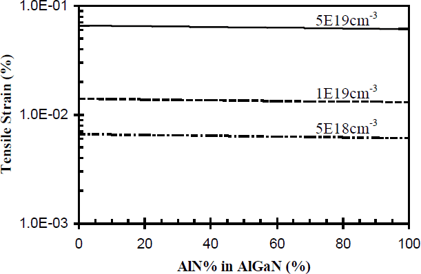
Figure 1. Si-doping induced strain as a function of mole fraction AlN in AlGaN. Si doping levels are as noted on the graph.
Figure 1 also indicates a slight decrease in the strain as the AlN mole fraction increases. This is a result of the AlN unit cell being smaller than the GaN unit cell and, thus, the Si substitutional impurity has less of an effect on the AlN lattice compared to the GaN lattice. The Si-doping strain increases with: 1. Increasing Si concentration and 2. Reducing AlN content of the AlGaN. The strain associated with doping GaN with 5E19cm−3Si is 0.066% and is tensile.
Discussion
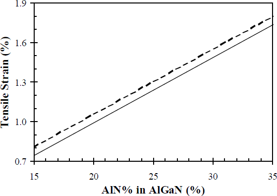
Of greater interest to HEMT structure design is how this effect manifests itself in a strained AlGaN / relaxed GaN system. Figure 2 is a graph of the strain associated with pseudomorphically strained AlGaN on relaxed GaN. If the AlGaN is doped with Si, the effect of the pseudomorphic and doping-induced strain is cumulative and increases the overall strain as shown by the dashed line of figure 2. The strain from incorporating 5E19cm-3 Si into the lattice is equivalent to increasing the AlN content in AlGaN by ∼1.4%. As the Si-doping level decreases, the dashed line would move closer to the solid line and the doping-induced strain would decrease as shown in figure 1.
In a modulation doped AlGaN/GaN HEMT, it is common practice to incorporate a thin undoped AlGaN spacer layer between the GaN and AlGaN:Si to spatially remove the ionized donors from the channel. The resulting structure is schematically shown in figure 3. A Ga-faced crystal structure is assumed which is the common polarity in metalorganic chemical vapor phase epitaxially grown GaN.Reference Ambacher, Smart, Shealy, Weimann, Chu, Murhpy, Schaff, Eastman, Dimitrov, Wittmer, Stutzmann, Rieger and Hilsenbeck 5 However, a similar argument could be made for a N-faced crystal.

Figure 2. Calculated strain for undoped AlGaN (solid line) and AlGaN:Si at a doping concentration of 5E19cm−3 (dashed line).
Figure 3 indicates the formation of the 2DEG at the AlGaN spacer layer / relaxed GaN layer interface. The sheet carrier concentration of the 2DEG depends on both the spontaneous and piezoelectric polarization associated with the AlGaN/GaN heterostructure. The additional lattice mismatch associated with the Si-doping will result in a second source of strain localized at the AlGaN:Si donor layer / AlGaN spacer layer interface. This strain manifests itself by the creation of an additional piezoelectric polarization in the AlGaN:Si donor layer. Due to the tensile nature of this strain, the resulting sheet charge will be positive. This additional sheet charge may accumulate at the AlGaN:Si/AlGaN interface resulting in a second 2DEG channel. The piezoelectric polarization associated with 5E19cm−3 Si is ∼0.35E12cm−2 which is an additional 1 – 4% of the polarization induce sheet charge generated by the AlxGa1−xN/GaN heterostructure (x is in the range of 0.15-0.35).

Figure 3. (a) modulation doped AlGaN/GaN HEMT structure and (b) the corresponding polarization fields. (Ga-faced crystal is assumed.)
Conclusions
Si-doping (Al)GaN causes a contraction of the wurtzite unit cell and can be a source of strain in doped AlGaN / GaN heterostructures. In a modulation doped AlGaN/GaN HEMT structure, in which the Si-doped AlGaN supply layer is separated from the 2DEG channel by an undoped AlGaN spacer layer, dopant-induced strain can create an additional source of charge at the AlGaN:Si/AlGaN interface. The magnitude of this strain increases as the Si doping concentration increases and the AlN mole fraction in the AlGaN decreases. The effect on the strain due to adding additional Si has a much greater effect than reducing the Al content in the AlGaN. Consideration of this strain should be given in AlGaN/GaN HEMT structure design.
Acknowledgements
Support for this research was provided by the U.S. Army Ballistic Missile Defense Organization and the Air Force.