


1. Introduction
Recent efforts in the development of III-V nitride semiconductors has led to the commercial production of high-brightness blue and green light-emitting diodes (LEDs) Reference Nakamura, Senoh, Iwasa, Nagahama, Yamada and Mukai[1] and to the demonstration of RT continuous wave (CW) laser diodes Reference Nakamura, Senoh, Nagahama, Iwasa, Yamada, Matsushita, Kiyoku and Sugimoto[2] Reference Nakamura[3]. Another application for nitride technology is e-beam pumped lasers for display technology Reference Basov, Dianov, Kozlovsky, Krysa, Nasibov, Popov, Prokhorov, Trubenko and Shcherbakov[4] [5]. The LCRT is promising as a stand alone projection display device Reference Nasibov, Kozlovsky, Reznikov, Skasyrsky and Popov[6] Reference Kozlovsky, Nasibov, Popov, Reznikov and Skasyrsky[7], as a high power light source for existing projection displays and as an ultraviolet light source for photolithography Reference Kamensky, Kozlovsky, Markov, Nasibov and Skasyrsky[8]. The LCRT would typically operate in a vertically pumped configuration. However, due to difficulty of fabricating suitable vertical cavity structures we have initially investigated in-plane laser cavities. Further studies are underway to prepare vertical cavity samples.
Short wavelength vertical cavity (VCL) electron beam pumped lasers have been demonstrated using II-VI bulk single crystal compounds: ZnSe (470 nm at RT) Reference Akimova, Dudenkova, Kozlovsky, Korostelin, Nasibov, Reznikov, Tishina and Shapkin[9], ZnO (375 nm at 80 K) Reference Kamensky, Kozlovsky, Markov, Nasibov and Skasyrsky[10], and ZnS (330 nm at 80 K) Reference Kozlovsky, Korostelin, Nasibov, Skasyrsky and Shapkin[11]. In the VCL geometry, RT thresholds are still too high for commercial applications of these devices. Significant reduction in the threshold current is expected when bulk active regions are replaced by heterostructures employing MQW active. Heterostructures in the II-VI ZnSe material system have been demonstrated (493 nm at RT) Reference Basov, Dianov, Kozlovsky, Krysa, Nasibov, Popov, Prokhorov, Trubenko and Shcherbakov[12] but they suffer from short lifetimes of several hours due to defect propagation. We believe that the III-V nitride compounds are ideally suited for short wavelength laser screens because of their greater thermal conductivity and superior stability under high excitation levels.
2. Experiment
The samples were grown by MOCVD on (0001) sapphire. The active region is composed of 30 In0.15Ga0.85N quantum wells with GaN barriers. The MQW region is surrounded by GaN waveguiding layers and AlGaN cladding layers. There is a In0.1Ga0.9N layer beneath the lower cladding to prevent cracking. In order to create laser cavities for e-beam pumping, the sapphire substrate was thinned. Rectangular bars were then scribed and cleaved. The bar width, which varies from 0.12 to 0.16 mm, is the cavity length. Different areas of the cavity may be independently excited along the bar length (5 -6 mm) depending on the position of the e-beam spot.
Surface emission was measured on as grown samples with low-power CW e-beam excitation: electron energy E e = 30 KeV, e-beam current I e = 1 μA and e-beam spot diameter d e = 1 mm. The prepared laser cavities were pumped in two different schemes: scanning and pulsed e-beam. Measurements were done at 80 K and RT. The scanning e-beam, typically used in VCL geometry, is required for projection display applications utilizing the LCRT. In this mode, the quasi-CW e-beam with 35 keV electron energy is scanned with a velocity v sc = 105 cm/s at 50 Hz along the bar length creating pulse excitation at each point along the bar with a time duration t = d e /V sc . Typically d e = 25-50 μm increasing with higher e-beam current from 0 to 2 mA. The pulsed e-beam source is a cold cathode with a blast emission and is not monochromatic. Although the maximum electron energy was 150 keV, the maximum current corresponds to 75 keV. Total current was approximately 500 A, the pulse duration was 1 ns and repetition rate was 1 Hz. The excitation area was formed by a metallic 100 μm - width split oriented perpendicular to the cleaved faces. The current density was calculated by dividing the current by the e-beam spot area. The emission was collected by a monochromator with a CCD array having 0.2 Å resolution.
Figure 1 shows emission at RT. For CW excitation, the MQW region shows emission at 409 nm, with 11 nm FWHM. A 120 μm laser bar was pumped by pulsed and scanning e-beam. The RT pulsed e-beam configuration showed strong stimulated emission at 409 nm, with 1.2 nm FWHM. The threshold current density was estimated to be 200-300 A/cm2. Stimulated emission associated with the In0.1Ga0.9N region is also observed. At RT, stimulated emission was not observed in the scanning e-beam configuration for the maximum current density of 100 A/cm2.

Figure 1. Emission spectra at RT
Testing at 80 K showed stimulated emission in the scanning mode configuration. The light output plotted versus e-beam current for a 160 μm cavity length is shown in Figure 2. A threshold current of 0.3 mA was measured corresponding to a current density of 60 A/cm2. Directly above threshold, the light increases linearly but becomes sublinear with higher currents. This is partly explained by the fact that the e-beam diameter increases with increasing current. Heating may also play a role in this sublinear behavior of the light output. At a current of 1.7 mA, the maximum output power of one facet was 150 mW.
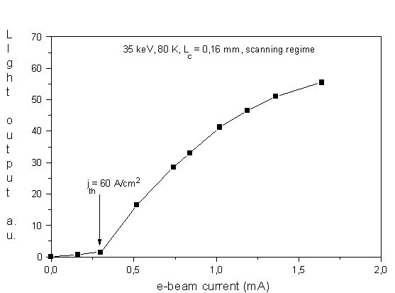
Figure 2. Light output versus e-beam current
At the threshold under scanned pumping the material gain g m is given by
where α is the internal loss, L c is the cavity length, ln(1/R) / Lc is the mirror loss, and G is the optical confinement factor. Taking de = 25 μm, L c = 160 μm, R = 0.22, α = 43 cm−1 from Reference Nakamura[3] and G = 0.085 (it is roughly equal to the relation of the total thickness of 30 QWs to the total thickness of the MQW active structure plus the thickness of the guiding layers) we obtain that g m = 104 cm−1 at T = 80. The actual g m is smaller because the excitation area is not restricted by the e-beam spot. At RT, laser action was achieved by pulse pumping when the e-beam spot (rectangular area) was larger than the cavity length. So, in the upper formula we should take d e = L c then we obtain that g m = 1600 cm−1. In any case gm > 103 cm−1 is too large to suggest that the mechanism of the stimulated emission is due to the localized carriers Reference Nakamura[3] having a wide emission line (54 - 89 meV) at low excitation.
Furthermore, taking into account that only about t = 1 μm from about ze = 4 μm of the excitation area depth at Ee = 35 keV is used for pumping of QWs, and the number of the nonequilibrium e - h pairs generated by one fast electron is E e /3 E g ≈ 3300 we can obtain that the e-beam pumping threshold (60 A/cm2 at 80 K) corresponds to the LD threshold per one QW as
This value would be smaller if the e-beam spot diameter would be equal to the cavity length. At RT and the pulse pumping t/Z e ≈ 0.035 and E e /3E g ≈ 15000 we obtain the following evaluation:
Taking into account that the used pulse duration is only 1 ns smaller than the carrier lifetime of 2-10 ns measured in Reference Nakamura[3] (it is really pulse excitation but not quasi CW one) the threshold for quasi CW excitation will be comparable with the one in Reference Nakamura[3].
We can estimate the threshold density of the e - h pairs in the QWs as
where e is the charge of electron. At RT we find that ρth(RT) = (2-3) * 1013 cm−2. This density is essentially greater than in GaAs and even ZnSe similar devices. The main reason is the micro inhomogeneity of InGaN layers leading to a creation of electron captures with a density of order 1013 cm−2. This is very good for an LED because the transport of carriers to defects is limited and high efficiency is realized by localized states. However, to achieve laser action we need to fill these electron captures at first and then create high-density e-h plasma to achieve a high gain.
3. Summary
E-beam pumping of an (In,Ga,Al)N in-plane laser heterostructure with an InGaN/GaN MQW active region was reported for the first time. Cleaved facet laser bars were prepared. At 80 K, lasing was demonstrated using a scanning electron beam of 35 keV electron energy. The e-beam threshold current density was 60 A/cm2 with a peak wavelength of 402 nm. Maximum light output of 150 mW was measured out of one facet. At RT, a pulsed e-beam with a maximum of 150 keV electron energy and 1 ns pulse duration was used. A lasing wavelength of 409 nm was measured and a threshold current density of 200-300 A/cm2.
Acknowledgments
We gratefully acknowledge the support of this effort by Academician Nikolai G. Basov of the P.N. Lebedev Physical nstitute and for his vision of electron beam stimulated lasers introduced in his 1964 Nobel Lecture, Professor Robert S. Feigelson of Stanford University and NASA's Jet Propulsion Laboratory. The University of California at Santa Barbara expresses their gratitude to the work sponsored by Dr. Anis Husain, DARPA grant N00014-96-1-0738.


