Introduction
Current intensive experimentation on III-V nitrides has led to rapid progress in blue light and high power device applications [Reference Strite and Morkoc1]. These achievements contrast greatly an apparent lack of good understanding of many fundamental issues related to growth and film properties of nitrides. To further improve the quality of epitaxial thin films and hereafter the performance of nitride-based optoelectronic and microelectronic devices, a better knowledge of its growth kinetics and surface dynamics is obviously needed.
In a non-equilibrium growth system such as molecular beam epitaxy (MBE), surface morphology contains important kinetic and dynamic information related to the growth process [Reference Zhang and Lagally2]. Therefore, by studying the morphological evolution of surfaces during MBE growth under various conditions, key kinetic parameters governing growth can be derived.
This paper presents recent observations of many novel morphologies during growth of GaN(0001) on SiC(0001) substrates without the use of buffer layers. Both nominally flat and vicinal substrates are used. In addition to the strong anisotropy in growth rates of two types of surface steps, step bunching during vicinal film growth is also observed. Furthermore, for a vicinal film, there is no spiral mound, which is the dominant feature for a flat surface.
Experiments
MBE growth and scanning tunneling microscopy (STM) experiments of GaN films are conducted in a multi-purpose ultrahigh vacuum (UHV) system, with background pressures in the range of 10−11 mbar. The MBE system is equipped with a conventional effusion cell for gallium (Ga) and a radio-frequency plasma generator for N2. For all the GaN growth reported in the paper, the Ga source temperature is set at 980°C, and the N2 flow rate at 0.13 sccm (standard cubic centimeter per minute). The power of the plasma unit is set at 500W. These conditions correspond to an III/V flux ratio of approximately 2 and a GaN growth rate of 0.26 Å s−1 [Reference Seutter, Xie, Zhu, Zheng, Wu and Tong3]. The substrates are nominally flat 6H-SiC(0001) (Cree Research, Inc.) and vicinal 4H-SiC(0001) (Nippon Steel, Co.) misoriented towards [-1010] by 3.5°. Prior to GaN deposition, the substrates are deoxidized at 1100°C in a Si flux supplied from an e-beam evaporator. The chemical purity of the treated surface is monitored by in situ X-ray photoelectron spectroscopy (XPS), while the atomic order of the surface is analyzed by in situ low energy electron diffraction (LEED). Under a properly chosen Si flux condition, the SiC surfaces show the (√3 × √3)R30° surface reconstruction following the deoxidization process. STM images of the surface show atomically flat terraces of more than 1000 Å wide for the flat substrate and a step-terrace morphology for the vicinal substrate. GaN growth is initiated by simultaneously opening the source shutters of Ga and N and at substrate temperatures between 500°C and 650°C. Sample heating is achieved by passing through it a direct current (DC) along the long side of the rectangular substrate pieces (11 × 4 mm2 in size).
To terminate growth, the source shutters are closed simultaneously and at the same time, the power of the plasma unit is switched off. Meanwhile, the sample is quenched rapidly by switching off the DC heating power. Due to the small sample size, the temperature drops quickly to below 400°C within seconds. The quenched surface is subsequently examined by in situ STM. Constant current mode STM experiments are conducted at room temperature at a tunneling current of 0.1nA and sample bias of -3V.
Results and Discussions
GaN growth on both flat and vicinal substrates commences by three-dimensional (3D) island formation as indicated by reflection high-energy electron diffraction (RHEED) patterns. This is followed by a transition to two-dimensional (2D) growth after coalescence of 3D islands. It is noted that such transition from 3D to 2D growth is sooner for the vicinal film than flat ones. Continued growth on the two substrates leads to completely different morphologies, which is the subject of the following discussion.
Flat Surface
Fig. 1(a) shows a GaN surface following 1µm deposition at 650°C. The main observation is the dominance of spiral mounds on the surface. The density of such mounds is estimated from the image to be 2 × 109 cm−2. As growth spirals originate from screw or mixed-type threading dislocations in the film [Reference Burton, Cabrera and Frank4], it is concluded that the density of screw threading dislocations in the flat film is of the order of 2 × 109 cm−2, which has been confirmed by transmission electron microscopy (TEM) investigations [Reference Xie, Zheng, Ng, Wu, Ohtani and Tong5]. Similar morphologies have also been reported by others [Reference Heying, Tarsa, Elsass, Fini, DenBaars and Speck6,Reference Smith, feenstra, Greve, Shin, Skowronski, Neugebauer and Northrup7], therefore, it seems that it is characteristic to MBE-grown GaN films on flat substrates. Note that if a pair of growth spirals originates from growth at two vertical screw arms of a ‘U’-shaped dislocation line, then the spirals in the pair ought to have opposite rotation direction. Indeed, both clockwise and anti-clockwise rotation spirals are seen.

Figure 1. STM images of GaN surfaces following deposition on flat SiC(0001) substrates at (a) and (b) 650°C, (c) 500°C. Note the scale difference between (a) and (b).
Zooming-in one of the spiral mounds reveals a special step structure, as shown in fig. 1(b). Along one of the <10-10> crystallographic directions, steps are all double bilayer (BL) high, i.e., it equals c = 5.2 Å, the height of the unit cell of GaN in the [0001] direction. In between the two adjacent double BL steps, along the [Reference Xie, Cheung, Zheng, Ng, Wu, Ohtani and Tong11-20] direction, the steps are de-paired into single BL and a twilled structure results. Such a step structure is understood by considering the dangling bond characteristics of a wurtzite film [Reference Xie, Seutter, Zhu, Zheng, Wu and Tong8]. For such a film’s surface, there are two types of steps, namely type-A and type-B steps. For a type-A step, each edge atom has two dangling bonds whereas for type-B steps, the edge atom has only one dangling bond. Therefore, for a type-A step, there is a high density of kinks whose advance is limited by the arrival rate of adatoms by diffusion. On the other hand, for a type-B step, there are few kinks, as the creation of a kink site on such a step will expose the high-energy type-A step. As a result, the motion of a type-B step may involve nucleation of one-dimensional (1D) islands along the step edge, therefore, its speed of growth is reduced compared to the growth of a type-A step. For a wurtzite film, consecutive steps along a given <10-10> direction belong to type-A and type-B alternately, therefore, the fast-growing type-A step will ultimately catch up with the slower-growing type-B step underneath, and step-pairing occurs. On the same terrace, a step changes its character from type-A to type-B or vice versa upon turning 60°. This explains the formation of the twilled structure of single BL steps along the [Reference Xie, Cheung, Zheng, Ng, Wu, Ohtani and Tong11-20] direction.
Under the island nucleation growth mode at low substrate temperatures, e.g., 500°C, 2D single BL height islands form on terraces that show triangular shape, as depicted in fig. 1(c). The triangular shape is again due to the growth anisotropy of GaN. The fast-growing type-A step ultimately makes this step disappear and the island becomes bounded by the slower-growing, low energy, type-B steps. Unexpectedly, from the image of fig. 1(c), triangular islands oriented 180° with respect to each other on the same terrace are seen. To explain this, we assume atoms in some of the islands are wrongly stacked. For example, instead of the wurtzite ABAB… stacking, atoms take the cubic ABCA… stacking instead. The oppositely oriented triangular islands can also originate from twins in a pure cubic film, i.e., one with ABCA… and the other with ACBA… stacking. It has been shown by TEM studies that low growth temperature promotes cubic film formation and there is a high density of stacking faults and twin boundaries in such a film [Reference Xie, Zheng and Tong9]. Therefore, the assertion of the 180°-oriented islands to stacking faults and twins is likely to be correct.
Vicinal Surface
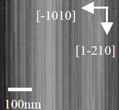
Fig. 2 shows a GaN surface following a 0.5µm film deposition at 650°C on a vicinal SiC substrate. The most remarkable difference between this surface and the flat one (fig. 1(a)) is the absence of spiral mounds. As described earlier, spiral mounds reflect growth at screw threading dislocations. Therefore, the absence of spirals in fig. 2 implies a suppression of threading screw dislocations in the vicinal film. This suggestion has been confirmed by TEM studies, which reveal a density of screw threading dislocation in the vicinal film of the order of 107 cm−2. This is two-orders of magnitude less than that in the flat film. In addition to screws, TEM images also suggest a reduction of threading edge dislocations. Therefore, judging by these results, the quality of the vicinal epitaxial film is substantially improved. The cause of dislocation suppression is still under investigation, preliminary results indicate that it is likely related to the initiation and coalescence processes of islands when GaN is initially grown on SiC. Examining the individual steps reveals they are all double BL high, in agreement with the growth anisotropy described earlier.

Figure 2. STM image of a GaN film grown on a vicinal 4H-SiC(0001) substrate at 650°C. Note the absence of spiral mounds.
Let’s now consider the implication of the above step structure to step kinetics during MBE growth. Referring to the 1D model of a vicinal GaN surface as shown in fig. 3, XA and XB denote the positions of steps A and B belonging to type-A and type-B, respectively. Let W be the terrace width bounded by the two steps, while W + and W - are the terrace widths in front of and behind the B and A steps, respectively (see fig. 3). If


Figure 3. A 1D model of a vicinal GaN surface. The consecutive steps belong to type-A and type-B, respectively, as required by the wurtzite crystal structure.
In writing down equ. (1), we have ignored the lateral fluctuations of steps. The two terms on the right-hand side of the equation reflect contributions from the upper and lower terraces, respectively. Subtract the two equations and note that W = XB − XA , one obtains

where we have used an approximation of W ≈ 0 in deriving the second equality. It is valid when step-pairing has occurred (i.e., A step has caught up with the B step) and so there is no terrace between the two steps. Note further that statistically, W + =W −, as the two terraces are equivalent. Therefore,

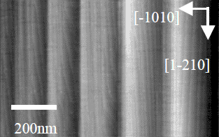
In order to maintain the double BL step (DBS) structure during growth, one requires
Once a DBS has formed, which constitutes an A step on top and a B step below, the motion of such a DBS ‘unit’ is determined by adatom incorporation from the upper terrace behind step A and from the lower terrace in front of step B. If, as argued above, the rate of incorporation of adatoms from the upper terrace is higher than that from the lower terrace, continued growth will lead to further step bunching [Reference Bennema, Gilmer and Hartman10]. A complication comes, however, from the fact that adatom incorporation at a DBS may be different than that of an adatom diffusing down a step. At a DBS, adatoms need to cascade two BL height steps, A and B, in order to be successfully incorporated in the step. On the other hand, step bunching following continued growth of the vicinal film has indeed been observed [Reference Xie, Cheung, Zheng, Ng, Wu, Ohtani and Tong11]. An example of a bunched surface is shown in fig. 4, which is obtained after GaN deposition for another 2.5µm on top of the surface given in fig. 2. It is further shown that the bunching behavior depends on the DC direction that is applied across the sample in order to maintain the substrate temperature. Step bunching occurs only when the electric field points to the step down direction of the vicinal surface. When the field is reversed, the bunched steps tend to debunch. This observation, therefore, points to the electromigration effect [Reference Xie, Cheung, Zheng, Ng, Wu, Ohtani and Tong11,Reference Latyshev, Aseev, Krasilnikov and Stenin12]. If so, according to the field dependence, we infer that adatoms, which are likely N in this case when the growth is under Ga-rich condition, possess effective positive charges. At the moment, it is not clear whether step bunching is caused solely by the electromigration effect, or it is also caused by a higher rate of incorporation of adatoms from the upper terrace compared to that from the lower terrace. More studies are needed to separate out these two effects.010]

Figure 4. STM image showing step bunching of the vicinal GaN film following prolonged growth at 650°C and heated by a DC along the step-down direction (from left to right).
Conclusions
We have summarized our observations of surface morphology of GaN during its MBE growth. A comparison is made between the flat and vicinal surfaces, where the former shows spirals mounds due to screw threading dislocations, contrasting to vicinal films where there is no spiral mound. This suggests an effective suppression of threading dislocations. Furthermore, strong growth anisotropy and step bunching are observed, which can have important implications in the design of nitride-based device structures.
Acknowledgements
This work is supported in part by HK RGC grants No. HKU7118/98P, 7117/98P, 7142/99P and 260/95P, US DOE grant No. DE-FG02-84ER 45076, US NSF grant No. DMR-9972958. The vicinal 4H-SiC substrate is kindly provided by Dr. N. Ohtani of Nippon Steel Corporation, Japan.