Hostname: page-component-78c5997874-lj6df Total loading time: 0 Render date: 2024-11-15T01:51:55.241Z Has data issue: false hasContentIssue false

Creation and Characterization of an Atomically Sharp Single/Trimer Atom Ir/W(111) Tip by Thermal Field-Assisted Faceting

Published online by Cambridge University Press:  23 July 2021
Kwang-Il Kim
Affiliation:
Scientific Instruments Platform Team, Advanced Instrumentation Institute, Korea Research Institute of Standards and Science (KRISS), 267 Gajeong-ro, Yuseong-gu, Daejeon 34113, South Korea Major in NanoScience, University of Science and Technology, 217 Gajeong-ro, Yuseong-gu, Daejeon 34113, South Korea
Junhyeok Hwang
Affiliation:
Scientific Instruments Platform Team, Advanced Instrumentation Institute, Korea Research Institute of Standards and Science (KRISS), 267 Gajeong-ro, Yuseong-gu, Daejeon 34113, South Korea Major in NanoScience, University of Science and Technology, 217 Gajeong-ro, Yuseong-gu, Daejeon 34113, South Korea
Min-Wook Pin
Affiliation:
Advanced Process and Materials R&D Group, Korea Institute of Industrial Technology (KITECH), 156 Gaetbeol-ro, Yeonsu-gu, Incheon 21999, South Korea
Jihwan Kwon
Affiliation:
EM Nanometrology Team, Interdisciplinary Materials Measurement Institute, Korea Research Institute of Standards and Science (KRISS), 267 Gajeong-ro, Yuseong-gu, Daejeon 34113, South Korea
Ha Rim Lee
Affiliation:
EM Nanometrology Team, Interdisciplinary Materials Measurement Institute, Korea Research Institute of Standards and Science (KRISS), 267 Gajeong-ro, Yuseong-gu, Daejeon 34113, South Korea
In-Yong Park*
Affiliation:
Scientific Instruments Platform Team, Advanced Instrumentation Institute, Korea Research Institute of Standards and Science (KRISS), 267 Gajeong-ro, Yuseong-gu, Daejeon 34113, South Korea Major in NanoScience, University of Science and Technology, 217 Gajeong-ro, Yuseong-gu, Daejeon 34113, South Korea
*
*Corresponding author: In-Yong Park, E-mail: inyong.park@kriss.re.kr
Get access

Abstract

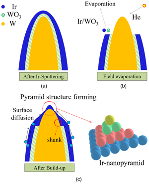
Atomically sharpened tips have attracted much interest in the imaging and manufacturing fields due to their high spatial resolutions. Typically, tungsten (W) is mainly used as the material of such a tip, but when the W tip is used in an oxygen environment, a limit is revealed due to corrosiveness stemming from a reaction with the oxygen gas. To solve this problem, methods of depositing a metal on W that does not react with oxygen have been studied. In this study, we introduce a method of depositing iridium (Ir) directly onto an insulating layer without an additional pretreatment to remove the insulating layer remaining on the W surface, forming an Ir-nanopyramid structure at the apex of the W tip by field evaporation and faceting. Field ion microscopy and atom probe tomography were used to analyze the crystal structure and composition at the apex during the faceting process, and the overall tip shape change after faceting was compared and analyzed with transmission electron microscopy. The proposed method does not have a tip heating step when creating an atomically sharp tip such that it can be made easily with a simpler equipment configuration than in the existing method.

Type
Materials Science Applications
Copyright
Copyright © The Author(s), 2021. Published by Cambridge University Press on behalf of the Microscopy Society of America

Access options

Get access to the full version of this content by using one of the access options below. (Log in options will check for institutional or personal access. Content may require purchase if you do not have access.)

References

Al Soud, A, Albuqain, R & Suleiman Mousa, M (2020). Composite metallic nano emitters coated With a layer of insulator covered by Au layer.Jordan Journal of Physics 13, 253262.Google Scholar
Al Soud, A, Knápek, A & Suleiman Mousa, M (2020). Analysis of the various effects of coating W tips with dielectric epoxylite 478 resin or UPR-4 resin coatings under similar operational conditions. Jordan Journal of Physics 13,191199.Google Scholar
Antczak, G, Błaszczyszyn, M & Błaszczyszyn, R (2000). Surface self-diffusion of iridium: Field electron emission study. Acta Phys Pol A 98, 383388.CrossRefGoogle Scholar
Bettler, PC & Charbonnier, FM (1960). Activation energy for the surface migration of tungsten in the presence of a high-electric field. Phys Rev 119, 8593.CrossRefGoogle Scholar
Binh, V & Marien, J (1988). Characterization of microtips for scanning tunneling microscopy. Surf Sci 202, L539L549.CrossRefGoogle Scholar
Demers, H, Poirier-Demers, N, , A, Couture, AL, Joly, D, Guilmain, M, De Jonge, N & Drouin, D (2011). Three-dimensional electron microscopy simulation with the CASINO Monte Carlo software. Scanning 33, 135146.CrossRefGoogle ScholarPubMed
Fu, T, Cheng, L, Nien, C & Tsong, T (2001). Method of creating a Pd-covered single-atom sharp W pyramidal tip: Mechanism and energetics of its formation. Phys Rev B 64, 113401.CrossRefGoogle Scholar
Fu, TY, Lin, YC, Kuo, HS, Hwang, IS & Tsong, TT (2007). Study of two types of Ir or Rh covered single atom pyramidal W tips. Surf Sci 601, 39923995.CrossRefGoogle Scholar
Gault, B, Moody, MP, Cairney, JM & Ringer, SP (2012). Atom probe crystallography. Mater Today 15, 378386.CrossRefGoogle Scholar
Gomer, R (1993). Field Emission and Field Ionization (AVS Classics of Vacuum Science and Technology). American Institute of Physics. Available at http://oz8shu9n3i56rao.s3.amazonaws.com/Field_Emissions_and_Field_Ionization_AVS_Classics_in_Vacuum_Science_and_Technology.pdf (Accessed July 3, 2020).Google Scholar
Gu, H, Li, G, Liu, C, Yuan, F, Han, F, Zhang, L & Wu, S (2017). Considerable knock-on displacement of metal atoms under a low energy electron beam. Sci Rep 7, 184.CrossRefGoogle Scholar
Guan, J, Campbell, RA & Madey, TE (1995). Ultrathin metal films on W(111): Morphology and faceting reconstruction. Surf Sci 341, 311327.CrossRefGoogle Scholar
Jeng, HT, Kuo, HS, Hwang, IS & Tsong, TT (2010). High stability and electronic structures of noble-metal covered W(111) atom perfect pyramidal tips. Phys Rev B 81, 155424.CrossRefGoogle Scholar
Kim, KI, Kim, YH, Ogawa, T, Choi, S, Cho, B, Ahn, SJ & Park, IY (2018). Fabrication of a trimer/single atom tip for gas field ion sources by means of field evaporation without tip heating. Ultramicroscopy 192, 5056.CrossRefGoogle ScholarPubMed
Kuo, HS, Hwang, IS, Fu, TY, Hwang, YS, Lu, YH, Lin, CY, Hou, JL & Tsong, TT (2009). A single-atom sharp iridium tip as an emitter of gas field ion sources. Nanotechnology 20, 335701.CrossRefGoogle ScholarPubMed
Kuo, HS, Hwang, IS, Fu, TY, Lin, YC, Chang, CC & Tsong, TT (2006). Noble metal/W(111) single-atom tips and their field electron and ion emission characterises. Jpn J Appl Phys Part 1: Regul Pap Short Notes 45, 89728983.CrossRefGoogle Scholar
Kuo, HS, Hwang, IS, Fu, TY, Wu, JY, Chang, CC & Tsong, TT (2004). Preparation and characterization of single-atom tips. Nano Lett 4, 23792382.CrossRefGoogle Scholar
Lai, W-C, Lin, C-Y, Chang, W-T, Li, P-C, Fu, T-Y, Chang, C-S, Tsong, TT & Hwang, I-S (2017). Xenon gas field ion source from a single-atom tip. Nanotechnology 28, 255301.CrossRefGoogle ScholarPubMed
Liao, Y (2013). Practical Electron Microscopy and Database. www.globalsino.com/EM/ (3544).Google Scholar
Michely, T, Besocke, KH & Teske, M (1988). A combined scanning tunnelling and field ion microscope. J Microsc 152, 7783.CrossRefGoogle Scholar
Moody, MP, Gault, B, Stephenson, LT, Marceau, RKW, Powles, RC, Ceguerra, AV, Breen, AJ & Ringer, SP (2011). Lattice rectification in atom probe tomography: Toward true three-dimensional atomic microscopy. Microsc Microanal 17, 226239.CrossRefGoogle ScholarPubMed
Muntifering, B, Dingreville, R, Hattar, K & Qu, J (2015). Electron beam effects during in-situ annealing of self-ion irradiated nanocrystalline nickel. In Materials Research Society Symposium Proceedings, vol. 1809, pp. 13–18. Materials Research Society. Available at https://link.springer.com/article/10.1557/opl.2015.499 (Accessed March 29, 2021).Google Scholar
Onoda, J & Mizuno, S (2011). Fabrication of <1 1 0> oriented tungsten nano-tips by field-assisted water etching. Appl Surf Sci 257, 84278432.CrossRefGoogle Scholar
Oshima, C, Tomitori, M, Shimoda, T, Yasaka, A, Asai, H, Rokuta, E, Kolodziej, JJ, Madey, TE, Keister, JW & Rowe, JE (2018). Conference ALC—‘17—Thermal stability of single-atom termination at a pyramidal apex of an Ir-W Tip*. Surf Sci Nanotechnol 21, 294297.CrossRefGoogle Scholar
Rahman, F, Onoda, J, Imaizumi, K & Mizuno, S (2008). Field-assisted oxygen etching for sharp field-emission tip. Surf Sci 602, 21282134.CrossRefGoogle Scholar
Rezeq, M, Pitters, J & Wolkow, R (2006). Tungsten nanotip fabrication by spatially controlled field-assisted reaction with nitrogen. J Chem Phys 124, 204716.CrossRefGoogle ScholarPubMed
Sakurai, T, Hashizume, T, Kamiya, I & Hasegawa, Y (1988). Combined field ion and scanning tunneling microscope. Available at http://avs.scitation.org/doi/pdf/10.1116/1.575128 (Accessed February 5, 2018).Google Scholar
Swanson, LW & Crouser, LC (1969). Angular confinement of field electron and ion emission. J Appl Phys 40, 47414749.CrossRefGoogle Scholar
Tsong, T (1992). Atom-Probe Field Ion Microscopy. Available at https://www.cambridge.org/core/journals/mrs-bulletin/article/book-reviews/8EFA32CD811FF50B996BD5B9B7B40336 (Accessed July 3, 2020).Google Scholar
Tsong, TT & Müller, EW (1970). Field adsorption of inert-gas atoms on field ion emitter surfaces. Phys Rev Lett 25, 911913.CrossRefGoogle Scholar
Vollnhals, F & Wirtz, T (2018). Correlative microscopy in 3D: helium Ion microscopy-based photogrammetric topography reconstruction combined with in situ secondary ion mass spectrometry. Anal Chem 90, 1198911995.CrossRefGoogle ScholarPubMed
Watanabe, M (2011). X-ray energy-dispersive spectrometry in scanning transmission electron microscopes. In Scanning Transmission Electron Microscopy, pp. 291351. New York, NY: Springer.CrossRefGoogle Scholar
Williams, DB & Carter, CB (2009). Scattering and diffraction. In Transmission Electron Microscopy, pp. 2338. USA: Springer.CrossRefGoogle Scholar
Wirtz, T, Dowsett, D & Philipp, P (2016). SIMS on the helium ion microscope: A powerful tool for high-resolution high-sensitivity nano-analytics. In Helium Ion Microscopy, pp. 297323. Springer Cham.CrossRefGoogle Scholar
Wood, JA, Urban, R, Salomons, M, Cloutier, M, Wolkow, RA & Pitters, JL (2016). Iridium single atom tips fabricated by field assisted reactive gas etching. Appl Surf Sci 367, 277280.CrossRefGoogle Scholar
Supplementary material: File

Kim et al. supplementary material

Kim et al. supplementary material

Download Kim et al. supplementary material(File)
File 691.5 KB