Hostname: page-component-77c89778f8-gq7q9 Total loading time: 0 Render date: 2024-07-19T10:41:53.625Z Has data issue: false hasContentIssue false

SEM Nano: An Electron Wave Optical Simulation for the Scanning Electron Microscope

Published online by Cambridge University Press:  22 February 2022

Surya Kamal
Affiliation:
NanoImaging Lab, Chester F. Carlson Center for Imaging Science, Rochester Institute of Technology, Rochester, NY14623, USA
Richard K. Hailstone*
Affiliation:
NanoImaging Lab, Chester F. Carlson Center for Imaging Science, Rochester Institute of Technology, Rochester, NY14623, USA
*
*Corresponding author: Richard K. Hailstone, E-mail: hailstone@cis.rit.edu
Get access

Abstract

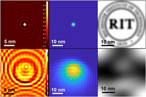
The simulation program “SEM Nano” is introduced to explain and visualize probe formation in field-emission scanning electron microscopes (SEMs). The program offers an easy and intuitive graphical user interface (GUI) to provide input in terms of understandable SEM parameters and visualization of the output. The simulations are based on wave optics treatment of the electron beam in the SEM column. Based on input parameters provided by the user, the spatial intensity distribution of electrons is calculated at the specimen by incorporating the effects of diffraction, aberrations, coherence, and noise. Given the specimen structure signal (So), the program has the capability to produce an image of the specimen using the electron probe intensity distribution. Finally, a feature is provided to reconstruct the electron probe intensity from the noisy image using a Wiener filter-based deconvolution.

Type
Software and Instrumentation
Copyright
Copyright © The Author(s), 2022. Published by Cambridge University Press on behalf of the Microscopy Society of America

Access options

Get access to the full version of this content by using one of the access options below. (Log in options will check for institutional or personal access. Content may require purchase if you do not have access.)

References

Barth, JE & Kruit, P (1996). Addition of different contributions to the charged particle probe size. Optik 101, 101109.Google Scholar
Barthel, J (2018). Dr. Probe: A software for high-resolution stem image simulation. Ultramicroscopy 193, 111.CrossRefGoogle ScholarPubMed
Bastiaans, MJ (1986). Application of the Wigner distribution function to partially coherent light. J Opt Soc Am A 3, 12271238.CrossRefGoogle Scholar
Born, M, Wolf, E, Bhatia, AB, Clemmow, PC, Gabor, D, Stokes, AR, Taylor, AM, Wayman, PA & Wilcock, WL (1999). Principles of Optics: Electromagnetic Theory of Propagation, Interference and Diffraction of Light, 7th ed. Cambridge: Cambridge University Press.CrossRefGoogle Scholar
Bronsgeest, MS, Barth, JE, Swanson, LW & Kruit, P (2008). Probe current, probe size, and the practical brightness for probe forming systems. J Vac Sci Technol B 26, 949955.CrossRefGoogle Scholar
Cremer, JT (2012). Chapter 3 - Geometric neutron and X-ray optics – aberrations. In Advances in Imaging and Electron Physics, vol. 172, Cremer JT (Ed.), pp. 429–495. Elsevier. Available at https://www.sciencedirect.com/science/article/pii/B9780123944221000037Google Scholar
Crewe, AV (1987). Optimization of small electron probes. Ultramicroscopy 23, 159167.CrossRefGoogle Scholar
Drouin, D, Couture, AR, Joly, D, Tastet, X, Aimez, V & Gauvin, R (2007). CASINO V2.42: A fast and easy-to-use modeling tool for scanning electron microscopy and microanalysis users. Scanning 29, 92101.CrossRefGoogle ScholarPubMed
Dubois, F, Requena, MLN, Minetti, C, Monnom, O & Istasse, E (2004). Partial spatial coherence effects in digital holographic microscopy with a laser source. Appl Opt 43, 11311139.CrossRefGoogle ScholarPubMed
Dwyer, C, Erni, R & Etheridge, J (2010). Measurement of effective source distribution and its importance for quantitative interpretation of stem images. Ultramicroscopy 110, 952957.CrossRefGoogle Scholar
Egerton, RF (2005). The Transmission Electron Microscope, pp. 5792. Boston, MA: Springer US.Google Scholar
Fransen, M, Van Rooy, TL, Tiemeijer, P, Overwijk, M, Faber, J & Kruit, P (1999). On the Electron-Optical Properties of the ZrO/W Schottky Electron Emitter, pp. 91166. Elsevier. Available at https://www.sciencedirect.com/science/article/pii/S1076567008702179Google Scholar
Fransen, MJ, Faber, JS, van Rooy, TL, Tiemeijer, PC & Kruit, P (1998). Experimental evaluation of the extended Schottky model for ZrO/W electron emission. J Vac Sci Technol B 16, 20632072.CrossRefGoogle Scholar
Gauvin, R, Lifshin, E, Demers, H, Horny, P & Campbell, H (2006). Win X-ray: A new Monte Carlo program that computes X-ray spectra obtained with a scanning electron microscope. Microsc Microanal 12, 4964.CrossRefGoogle ScholarPubMed
Gbur, G & Visser, T (2010). Chapter 5 - The structure of partially coherent fields, pp. 285–341. Elsevier. Available at https://www.sciencedirect.com/science/article/pii/B9780444537058000059Google Scholar
Goodman, JW (2017). Introduction to Fourier Optics, 4th ed., Vol. 1. New York: W.H. Freeman.Google Scholar
Haider, M, Uhlemann, S & Zach, J (2000). Upper limits for the residual aberrations of a high-resolution aberration-corrected stem. Ultramicroscopy 81, 163175.CrossRefGoogle ScholarPubMed
Hanssen, KJ & Trepte, L (1971). The influence of voltage and current fluctuations and of finite energy width of the electrons on contrast and resolution in electron microscopy. Optik 32, 519538.Google Scholar
Hawkes, P & Kasper, E (2018 a). Chapter 43 - General features of electron guns. In Principles of Electron Optics, 2nd ed., Hawkes P & Kasper E (Eds.), pp. 1051–1061. Academic Press. Available at https://www.sciencedirect.com/science/article/pii/B9780128133699000439.CrossRefGoogle Scholar
Hawkes, P & Kasper, E (2018 b). Chapter 44 - Theory of electron emission. In Principles of Electron Optics, 2nd ed., Hawkes P & Kasper E (Eds.), pp. 1063–1081. Academic Press. Available at https://www.sciencedirect.com/science/article/pii/B9780128133699000440CrossRefGoogle Scholar
Jon, OE (2009). Handbook of Charged Particle Optics, 2nd ed., pp. 391435. Boca Raton, FL: CRC Press.Google Scholar
Kandel, Y, Zotta, M, Caferra, A, Moore, R & Lifshin, E (2015). Measurement of the electron beam point spread function (PSF) in a scanning electron microscope (SEM). Microsc Microanal 21, 699700.CrossRefGoogle Scholar
Krivanek, O, Dellby, N & Lupini, A (1999). Towards sub-Å electron beams. Ultramicroscopy 78, 111.CrossRefGoogle Scholar
Latychevskaia, T (2017). Spatial coherence of electron beams from field emitters and its effect on the resolution of imaged objects. Ultramicroscopy 175, 121129.CrossRefGoogle ScholarPubMed
Madan, I, Vanacore, GM, Gargiulo, S, LaGrange, T & Carbone, F (2020). The quantum future of microscopy: Wave function engineering of electrons, ions, and nuclei. Appl Phys Lett 116, 230502. doi:10.1063/1.5143008CrossRefGoogle Scholar
Nellist, P & Rodenburg, J (1994). Beyond the conventional information limit: the relevant coherence function. Ultramicroscopy 54, 6174.CrossRefGoogle Scholar
Nevins, MC, Zotta, MD, Hailstone, RK & Lifshin, E (2018). Visualizing astigmatism in the SEM electron probe. Microsc Microanal 24, 604605.CrossRefGoogle Scholar
Reimer, L (2000). Scanning electron microscopy: Physics of image formation and microanalysis, second edition. Measurement Science and Technology 11, 1826.CrossRefGoogle Scholar
Riháček, T, Horák, M, Schachinger, T, Mika, F, Matějka, M, Krátký, S, Fořt, T, Radlička, T, Johnson, C, Novák, L, Sed'a, B, McMorran, B & Müllerová, I (2021). Beam shaping and probe characterization in the scanning electron microscope. Ultramicroscopy 225, 113268.CrossRefGoogle ScholarPubMed
Sato, M (2011). Properties of the imaging performance of an electron optical system for SEM. Nucl Instrum Methods Phys Res A 645, 7478.CrossRefGoogle Scholar
Shiloh, R, Lu, PH, Remez, R, Tavabi, AH, Pozzi, G, Dunin-Borkowski, RE & Arie, A (2019). Nanostructuring of electron beams. Phys Scr 94, 034004. doi:10.1088/1402-4896/aaf258CrossRefGoogle Scholar
Tiemeijer, P, Mul, P, Freitag, B, Kujawa, S & Ringnalda, J (2005). Breaking the spherical and chromatic aberration barrier in transmission electron microscopy. Ultramicroscopy 102, 209214.Google Scholar
Typke, D & Dierksen, K (1995). Determination of image aberrations in high-resolution electron microscopy using diffractogram and cross-correlation methods. Optik 99, 155166.Google Scholar
Verbeeck, J, Tian, H & Schattschneider, P (2010). Production and application of electron vortex beams. Nature 467, 301304.CrossRefGoogle ScholarPubMed
Voelz, D (2011). Computational fourier optics: A MATLAB tutorial.CrossRefGoogle Scholar
Wirth, J (2019). Point spread function and modulation transfer function engineering. PhD Thesis. Rochester Institute of Technology. Available at https://scholarworks.rit.edu/theses/10227Google Scholar
Xiao, X & Voelz, D (2006). Wave optics simulation approach for partial spatially coherent beams. Opt Exp 14, 69866992.CrossRefGoogle ScholarPubMed
Zhang, L, Garming, MW, Hoogenboom, JP & Kruit, P (2020). Beam displacement and blur caused by fast electron beam deflection. Ultramicroscopy 211, 112925.CrossRefGoogle ScholarPubMed
Zotta, M, Jois, S, Dhakras, P, Rodriguez, M & Lee, J (2019). Direct measurement of the electron beam spatial intensity profile via carbon nanotube tomography. Nano Lett 19, 44354441.CrossRefGoogle ScholarPubMed
Zotta, M & Lifshin, E (2017). Scanning electron microscope point spread function determination through the use of particle dispersions. Microsc Microanal 23, 124125.CrossRefGoogle Scholar
Zotta, M, Nevins, M, Hailstone, R & Lifshin, E (2018). The determination and application of the point spread function in the scanning electron microscope. Microsc Microanal 24, 396405.CrossRefGoogle ScholarPubMed