


No CrossRef data available.
Article contents
A Simple Approach for Thickness Measurements Using Electron Probe Microanalysis
Published online by Cambridge University Press: 15 February 2021
Abstract
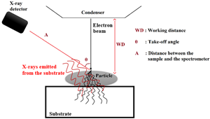
A simple and fast method for thickness measurements using electron probe microanalysis (EPMA) is described. The method is applicable on samples with a thickness smaller than the electron depth range and does not require any knowledge of instrumental parameters. The thickness is determined by means of the distance that electrons travel inside the sample before crossing through it. Samples are first deposited on a substrate that, when reached by the transmitted electrons, produces an X-ray signal. The measured characteristic X-ray line intensity of the substrate is later used to determine the energy of transmitted electrons, which is proportional to the distance that electrons travel inside the sample. The study was performed on spherical K411 glass particles and cylindrical particles of U–Ce oxide with a size ranging from 0.2 to 4 μm. The measured thicknesses of all the studied particles showed good agreements with the real values. Although the method is only validated on particles with usual shapes, it can be applied to determine a local thickness of thin samples with irregular morphologies. This can help solving multiple issues in analysis with EPMA of non-bulk samples exhibiting complex geometries. Three dimensional microscopic imaging could also find a good utility in the described method.
Keywords
- Type
- Software and Instrumentation
- Information
- Copyright
- Copyright © The Author(s), 2021. Published by Cambridge University Press on behalf of the Microscopy Society of America
References
Armstrong, JT (1991). Quantitative elemental analysis of individual microparticles with electron beam instruments. In Electron Probe Quantitation, Heinrich, KFJ & Newbury, DE (Eds.), pp. 261–315. New York, USA: Plenum Press.CrossRefGoogle Scholar
August, HJ & Wernisch, J (1987). A method for determining the mass thickness of thin films using electron probe microanalysis: Determination of mass thickness using EPMA. Scanning 9, 145–155.CrossRefGoogle Scholar
Delille, D, Pantel, R & Van Cappellen, E (2001). Crystal thickness and extinction distance determination using energy filtered CBED pattern intensity measurement and dynamical diffraction theory fitting. Ultramicroscopy 87, 5–18.CrossRefGoogle ScholarPubMed
Egerton, RF & Cheng, SC (1987). Measurement of local thickness by electron energy-loss spectroscopy. Ultramicroscopy 21, 231–244.CrossRefGoogle Scholar
Essani, M, Brackx, E & Excoffier, E (2020 a). A method for the correction of size effects in microparticles using a peak-to-background approach in electron-probe microanalysis. Spectrochim Acta B 169, 105880.CrossRefGoogle Scholar
Essani, M, Brackx, E, Pointurier, F, Berthy, F, Excoffier, E & Jonnard, P (2020 b). Characterization of the chemical composition of uranium microparticles with irregular shapes using standardless electron probe microanalysis and micro-Raman spectrometry. Anal Chem 92, 8435–8443.CrossRefGoogle ScholarPubMed
Green, M & Cosslett, VE (1961). The efficiency of production of characteristic X-radiation in thick targets of a pure element. Proc Phys Soc 78, 1206–1214.CrossRefGoogle Scholar
Groeber, MA, Haley, BK, Uchic, MD, Dimiduk, DM & Ghosh, S (2006). 3D reconstruction and characterization of polycrystalline microstructures using a FIB–SEM system. Mater Charact 57, 259–273.CrossRefGoogle Scholar
Guillaume, FB, Dijkstra, JM, Heijligers, HJM & Dick, K (1992). Quantitative electron probe microanalysis of multi-layer structures. In Electron Microbeam Analysis, Boekestein, A & Pavićević, MK (Eds.), pp. 93–97. Vienna: Springer Vienna.Google Scholar
Hauss Monteiro, DD, Limborço, H, Porto, RG, Moreira, AN, Rodrigues, WN & Magalhães, CS (2020). Metallization and Ar-O plasma effects on dental enamel roughness evaluated with SEM and MeX™ for 3D reconstruction. Microsc Res Tech 83, 597–603.CrossRefGoogle ScholarPubMed
Hombourger, C, Jonnard, P, Bonnelle, C & Staub, P-F (2003). Depth profiling of P shallow implants in silicon by electron-induced X-ray emission spectroscopy. Eur Phys J Appl Phys 24, 115–119.CrossRefGoogle Scholar
Hombourger, C, Jonnard, P, Filatova, EO & Lukyanov, V (2002). Thickness determination of very thin SiO2 films on Si by electron-induced x-ray emission spectroscopy. Appl Phys Lett 81, 2740–2742.CrossRefGoogle Scholar
Iakoubovskii, K, Mitsuishi, K, Nakayama, Y & Furuya, K (2008). Thickness measurements with electron energy loss spectroscopy. Microsc Res Tech 71, 626–631.CrossRefGoogle ScholarPubMed
Kanaya, K & Okayama, S (1972). Penetration and energy-loss theory of electrons in solid targets. J Phys D: Appl Phys 5, 43–58.CrossRefGoogle Scholar
Llovet, X & Merlet, C (2010). Electron probe microanalysis of thin films and multilayers using the computer program XFILM. Microsc Microanal 16, 21–32.CrossRefGoogle ScholarPubMed
Malis, T, Cheng, SC & Egerton, RF (1988). EELS log-ratio technique for specimen-thickness measurement in the TEM. J Electron Microsc Tech 8, 193–200.CrossRefGoogle ScholarPubMed
Mitchell, DRG (2006). Determination of mean free path for energy loss and surface oxide film thickness using convergent beam electron diffraction and thickness mapping: A case study using Si and P91 steel. J Microsc 224, 187–196.CrossRefGoogle ScholarPubMed
Oxford Instruments (n.d.). AZtec Layer probe. Available at https://nano.oxinst.com/products/aztec/layerprobe.Google Scholar
Pereyra, GD, Oliva, FY, Budini, N, Risso, G, Pérez, PD, Suárez, S & Trincavelli, JC (2020). Standardless determination of nanometric thicknesses in stratified samples by electron probe microanalysis. Spectrochim Acta B 171, 105932.CrossRefGoogle Scholar
Pouchou, JL & Pichoir, F (1990). Surface film X-ray microanalysis: Surface film x-ray microanalysis. Scanning 12, 212–224.CrossRefGoogle Scholar
Shi, S, Sun, S, Andrews, SB & Leapman, RD (1996). Thickness measurement of hydrated and dehydrated cryosections by EELS. Microsc Res Tech 33, 241–250.3.0.CO;2-T>CrossRefGoogle ScholarPubMed
Sweeney, WE, Seebold, RE & Birks, LS (1960). Electron probe measurements of evaporated metal films. J Appl Phys 31, 1061–1064.CrossRefGoogle Scholar
Tafti, AP, Kirkpatrick, AB, Alavi, Z, Owen, HA & Yu, Z (2015). Recent advances in 3D SEM surface reconstruction. Micron 78, 54–66.CrossRefGoogle ScholarPubMed
Titze, B & Genoud, C (2016). Volume scanning electron microscopy for imaging biological ultrastructure: Volume scanning electron microscopy. Biol Cell 108, 307–323.CrossRefGoogle ScholarPubMed
Wuttke, J (n.d.). lmfit – A C library for Levenberg-Marquardt least-squares minimization and curve fitting. Version v 8.3.0. Available at https://jugit.fz-juelich.de/mlz/lmfit.Google Scholar
Zhang, H-R, Egerton, RF & Malac, M (2012). Local thickness measurement through scattering contrast and electron energy-loss spectroscopy. Micron 43, 8–15.CrossRefGoogle ScholarPubMed