Hostname: page-component-586b7cd67f-rdxmf Total loading time: 0 Render date: 2024-11-30T04:43:21.649Z Has data issue: false hasContentIssue false

Photoemission Electron Microscopy as a New Tool to Study the Electronic Properties of 2D Crystals and Inhomogeneous Semiconductors

Published online by Cambridge University Press:  04 August 2017

Taisuke Ohta
Affiliation:
Sandia National Laboratories, Albuquerque, New Mexico, United States. Center for Integrated Nanotechnologies, Sandia National Laboratories, Albuquerque, New Mexico, United States.
Morgann Berg
Affiliation:
Sandia National Laboratories, Albuquerque, New Mexico, United States. Center for Integrated Nanotechnologies, Sandia National Laboratories, Albuquerque, New Mexico, United States.
Kunttal Keyshar
Affiliation:
Department of Materials Science and Nanoengineering, Rice University, Houston, Texas, United States Los Alamos National Laboratory, Los Alamos, New Mexico, United States.
Jason M. Kephart
Affiliation:
Department of Mechanical Engineering, Colorado State University, Fort Collins, Colorado, United States.
Thomas E. Beechem
Affiliation:
Sandia National Laboratories, Albuquerque, New Mexico, United States.
Robert Vajtai
Affiliation:
Department of Materials Science and Nanoengineering, Rice University, Houston, Texas, United States
Pulickel Ajayan
Affiliation:
Department of Materials Science and Nanoengineering, Rice University, Houston, Texas, United States
Aditya D. Mohite
Affiliation:
Center for Integrated Nanotechnologies, Sandia National Laboratories, Albuquerque, New Mexico, United States. Los Alamos National Laboratory, Los Alamos, New Mexico, United States.
Walajabad S. Sampath
Affiliation:
Department of Mechanical Engineering, Colorado State University, Fort Collins, Colorado, United States.
Calvin Chan
Affiliation:
Sandia National Laboratories, Albuquerque, New Mexico, United States.

Abstract

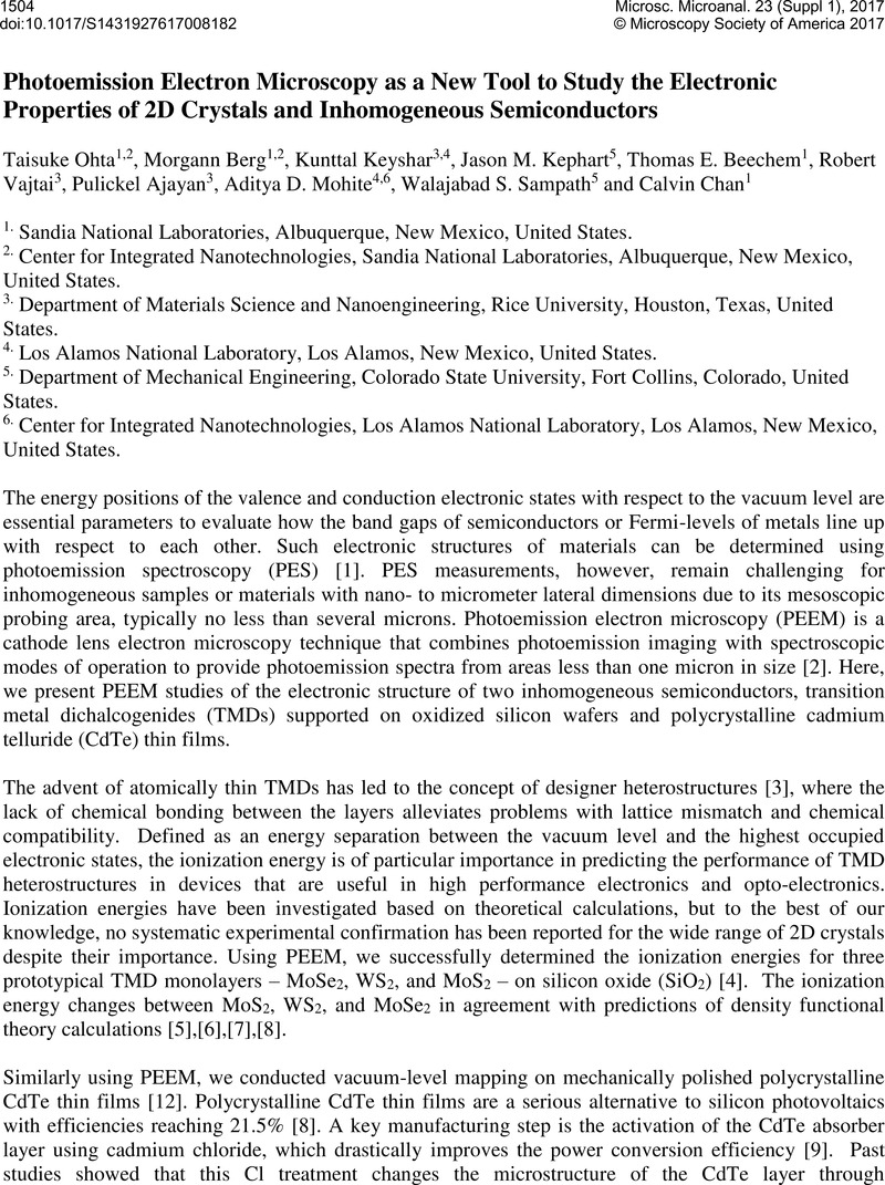
Image of the first page of this content. For PDF version, please use the ‘Save PDF’ preceeding this image.'
Type
Abstract
Copyright
© Microscopy Society of America 2017 

References

[1] Hufner, S in Photoelectron Spectroscopy, Principles and Applications. Springer Berlinp. 347.Google Scholar
[2] Bauer, E in Surface Microscopy with Low Energy Electrons. Springer New Yorkp. 25.Google Scholar
[3] Geim, A K & Grigorieva, I V Nature 499 2013). p. 419.CrossRefGoogle Scholar
[4] Keyshar, K, et al, in preparation (2017).Google Scholar
[5] Ataca, C, et al, J. Phys. Chem. C 116 2012). p. 8983.CrossRefGoogle Scholar
[6] Kang, J, et al, Applied Physics Letters 102 2013). p. 012111.CrossRefGoogle Scholar
[7] Gong, C, et al, Appl. Phys. Lett 103 2013). p. 053513.CrossRefGoogle Scholar
[8] Green, M A, et al, Prog. Photovoltaics 24 2016). p. 3.CrossRefGoogle Scholar
[9] Rasmussen, F A & Thygesen, K. S. J. Phys. Chem. C 119 2015). p. 13169.CrossRefGoogle Scholar
[10] Moutinho, H R., et al, J. Vacuum Science & Technology A 16 1998). p. 1251.CrossRefGoogle Scholar
[11] Visoly-Fisher, I, et al, Advanced Functional Materials 16 2006). p. 649.CrossRefGoogle Scholar
[12] Berg, M, et al, in preparation 2017.Google Scholar
[13] The PEEM work was performed at the Center for Integrated Nanotechnologies, an Office of Science User Facility (DE-AC04-94AL85000). T. O. was supported by the CINT user program and Sandia LDRD. M. B. and C. C. were supported by a U.S. DOE-EERE SunShot BRIDGE award (DE-FOA-0000654 CPS25859). K. K. was supported by the Army Research Office MURI (W911NF-11-1-0362). A. D. M. was supported by LANL LDRD. J. M. R. and W. S. S. were supported by NSF PFI:AIR-RA (#1538733). We thank R. Guild Copeland for constructing the tunable DUV light source, and Norman Bartelt for fruitful discussions. We also thank Anthony McDonald for providing photoluminescence maps of the TMD samples. Sandia National Laboratories is a multi-program laboratory managed and operated by Sandia Corporation, a wholly owned subsidiary of Lockheed Martin Corporation, for the U.S. Department of Energy’s National Nuclear Security Administration under contract DE-AC04-94AL85000.Google Scholar