


A New Decade of Innovation
Ten years is the typical lifetime for many scientific instruments, including atomic force microscopes (AFMs). Over the course of a decade, the capabilities and features of existing instruments often foretell the research strategy for the coming decade and identify the needs for the technology to advance. In the AFM industry, automation and improving the user interface and ease of operation are key features for instruments of the future. The current goal in pioneering the user interface for AFM automation is to ensure that the next generation of AFM instruments will support other long-established microscopy industries such as electron and optical microscopes. As with the Park XE- and NX-series instruments, the new FX-series AFM will provide an instrument to address applications previously dominated by other measurement technologies.
Is AFM Easy to Use?
The primary objective of AFM is to simultaneously measure three-dimensional surface topography and other physical properties, both reliably and repeatably, with sub-nanometer resolution. Sample preparation is nominal, if required at all, and the cost of ownership is much lower than related techniques. Therefore, AFMs are now considered indispensable tools in industrial and research applications. Large-scale acceptance of AFM, however, was initially restrained by complex operational knowledge that was often required of new users before they were comfortable with operating an AFM and could trust the data they obtained.
Although commercial AFMs have improved over time, AFM is still hard to learn and operate for many new users with no previous experience. Historically, sometimes tedious experimental setup and manual input by the investigator were required for AFM operation. Before acquiring any AFM data, a user must choose an appropriate probe, mount it (often using tweezers), and then manually align the optical detection system and viewing optics. Following these steps, a sample must be loaded, typically with one or more areas selected for imaging and analysis. The user must then select an imaging mode, tune the system, and carefully bring the tip into feedback before proceeding to image the sample surface. To acquire valid surface information, the user must then make several adjustments to ensure that the AFM properly tracks the sample surface. These potentially complex procedures have prevented AFM from becoming a mainstream technology, as it usually requires someone with great experience to obtain good, reproducible data.
Improved user convenience and enhanced performance are two factors that separate the new Park Systems FX-series AFMs from other AFM instruments. Improved user convenience is achieved by making primary operational steps motorized and automated. Better performance, on the other hand, indicates improved specifications and additional (or new) capabilities that provides a justifiable benefit to the user. While AFM manufacturers are competing on scan speed, resolution, and even lattice imaging, automation is often requested by the AFM community, and this has the greatest potential to expand the research applications and capacity of the AFM market (Figure 1).

Figure 1: How Park Systems will contribute to market needs of the AFM industry. Automation is a major criterion, followed by system performance and resolution. Other agenda items such as lattice imaging and scan speed are considered for specific sample and measurement needs.
“The Dream Machine Project”
Development of the automation was a dream machine project, with the objective of designing and producing an AFM that optimizes user convenience while introducing new features and enhanced performance. From the initial stage of product design, user convenience enhancements were to include full automation of probe exchange, beam alignment, and sample positioning. Performance-wise, the system noise floor, servo performance, and optical vision were improved from the previous generation of instruments. Development of the FX40 was built upon the experience acquired using crosstalk elimination technology used in the previous generations of Park AFMs [Reference Kwon1].
Figure 2 illustrates the basic structure of Park instruments that use two dedicated, completely independent flexure scanners, one for sample (XY) and the other for probe (Z) movement. By implementing this scanner design, the raw out-of-plane-motion (OPM) prior to image correction is less than 2 nm over an 80 μm scan range, facilitating precise measurements from raw sample data and negating the need for software leveling corrections that render measurements less reliable. The optical microscope assembly is fixed in the system's center, and the AFM head is located along its center axis and moves with the Z stage. The sample chuck and the XY scanner on the XY stage are located directly beneath the AFM head. The optical microscope assembly is fixed to the focus stage and can move vertically. In contrast to the NX-series AFM system, the focus stage is not fixed to the Z stage but separately rides on an optics stage. Such an arrangement limits the weight on the Z stage, making the system more stable and immune to external vibrations. A more robust Z stage, built on a high stiffness cross-roller guide and two bearing blocks, results in a lower mechanical noise floor than previous AFM systems. Furthermore, the optics stage moves the optical microscope assembly in the XY plane, a design consideration crucial for AFM automation.

Figure 2: Front view of the Park FX40. The view on the right reveals some major components normally hidden by the microscope housing.
The main elements of the FX40 optical microscope assembly are equivalent to XE- and NX- instruments and include an objective lens, tube lens, camera, and LED light source for optical vision (Figure 3). The main difference is a fiber-coupled super-luminescent diode (SLD) located on the side port of the optical microscope assembly. The objective lens focuses the SLD beam onto the AFM cantilever and fixes its position at the center of the optical view. This allows creation of an extremely small target beam spot size, facilitating the use of a broad range of cantilever sizes and applications.

Figure 3: The optical microscope assembly is decoupled from the moving plate of the Z stage, reducing the total Z-stage mass. A fiber coupled SLD is attached to the optical microscope assembly. The SLD beam is focused through the objective lens and always fixed at the center of the optical view.
Optical vision quality, a crucial component of industrial automation, is significantly enhanced compared to the NX-series AFMs. In the FX AFM head design, all elements of obstruction, such as a beam splitter, present in earlier designs were eliminated to optimize the optical beam path, resulting in resolution of line with a width of less than 1 μm (Figure 4).

Figure 4: Focusing the SLD beam through an objective lens results in a small beam spot on the back of the cantilever for improved performance. The updated FX optics can resolve 0.87 μm linewidth. PPP-NCHR is a commercial AFM probe from Nanosensors.
New Features
The FX40 has a sophisticated AFM design and interface with the goal of maximizing user convenience. State-of-the-art automation, which includes automatic probe exchange and SLD beam alignment using pattern recognition, is the primary design feature that facilitates system operation. Inside the FX40 are three camera modules: a primary view camera located at the system center, a sample view camera located on the left side of the system, and a QR code reader located on the right side. An eight-probe automatic tip exchanger (ATX) module is situated on the right side of the XY stage, and a sliding protective cover prevents foreign objects from falling into the ATX module when it is not in use (Figure 5).

Figure 5: The main components of the FX40 system include the ATX module (shown on the right) and three camera modules: a primary tip/sample view, a wide-angle sample view, and a QR code reader.
Probe Loading
Probe loading is the biggest obstacle for novice AFM users. The NX- and XE-series AFM systems addressed such challenges by using pre-mounted probes [2]. In the FX40, new probes can be automatically exchanged safely and easily from an 8-probe cassette (Figure 6). Once the probe cassette is placed onto the ATX module, the probes may be exchanged automatically onto the AFM head. The user can also replace individual probes manually and mount them onto a probe hand, as with previous systems.

Figure 6: Probe cassette exchange entails placing an 8-probe cassette atop the ATX module and unscrewing the locking knob to open the cassette cover.
Probe Exchange
Much like the automatic probe exchange on Park's industrial inline AFMs, probes are collected by a magnetic force control mechanism [3]. The QR code reader identifies the probe ID and the status of ATX slots. A vision recognition-based machine learning algorithm automatically tracks if probes are loaded onto their assigned positions in the ATX cassette and produces a status report if an error is detected during probe loading (Figure 7). The machine learning algorithm analyzes and tracks factors, such as the shape of the chip carrier and the loading position, to monitor and control successful or unsuccessful routines. This generates improved loading success rates.

Figure 7: Automatic detection of probe loading position. Smart vision recognition with a machine learning algorithm locates the position of a loaded probe.
The QR code imprinted on the chip carrier of each probe includes information for probe identification, including the serial number and probe type (Figure 8). With this information, the physical probe properties, such as cantilever geometry, drive percentages, quality factor, resonant frequency, spring constant, and tip geometry, can be accessed from a database. Once identification of the probes has been conducted, the operator can choose an appropriate probe to use, and the instrument selects a probe automatically from the cassette. Subsequently, the system finds and mounts the cantilever, and the SLD and photodetector are automatically aligned.

Figure 8: The QR code reader identifies the probe type by reading the QR codes on the chip carriers in the probe cassette.
Beam Alignment
With the new automated beam alignment, the SLD beam position is automatically aligned for precise, optimal positioning onto a cantilever. The SLD is fixed to the optical microscope assembly, and the SLD beam is permanently fixed at the center of the optical microscope. Using the XY motor adjustments of the optics stage, the cantilever can be positioned at the center of the optical view, and the SLD beam is automatically positioned onto the back of the cantilever. Based on the machine learning of a probe pattern, the position of the probe is detected by vision recognition (Figure 9).

Figure 9: Due to the fixed position of the SLD, whose beam path is shown in the red line, centering the cantilever in the middle of the optics immediately aligns the SLD. The SLD beam emerging from the objective lens is focused onto the optimal location on the PSPD, evidenced by the centering blue circle on the PSPD.
The SLD beam that emerges from the objective lens is automatically positioned onto the cantilever and reflected onto a position-sensitive photodetector (PSPD) using a steering mirror. To complete alignment of the beam-bounce, two motors within the FX AFM head modify the angle of the SLD beam steering mirror to point the SLD beam onto the optimal location on the PSPD. This level of automation eliminates user error during the complex beam alignment process and guarantees faultless, precise alignment (Figures 9 and 10).

Figure 10: The new motorized FX AFM head optimizes the SLD beam spot position on the PSPD both vertically and laterally for optimal operation.
Sample Navigation
The FX40 system is equipped with a multi snap-in sample chuck (Figure 11). Users can populate the sample chuck by taking advantage of four kinematically mounted sample plates. In both X and Y, the positioning repeatability of the sample disks is 5 μm. Using four sample plates with repeatable positioning facilitates comparison between reference and target samples for measurements that may include KPFM (kelvin probe) work function, PinPointTM nano-mechanics, SCM (scanning capacitance) dopant concentration, or scanning thermal microscopy (SThM) analysis.

Figure 11: The multi snap-in sample chuck is the default sample chuck for the FX40. The discs are kinematically mounted to ensure mounting repeatability.
A low-magnification sample view camera is used to assist the operator in navigating to the imaging location desired (Figure 12). As the user selects positions on the optical view screen, the clicked position of the XY stage coordinate is recognized, and the XY stage moves to locate the required measurement position directly beneath the probe tip. For precise navigation on an individual sample, it is possible to use the high-resolution optical view from the on-axis main view camera. Once sample navigation is completed, the cantilever then approaches the selected sample location automatically. For rapid engagement to sample surface, the sample height is measured by an innovative autofocus module. The tip approach is assisted by monitoring the effect of air damping while the probe approaches the sample surface. The vibration amplitude of the cantilever decreases monotonically and then linearly until the interatomic force draws the tip to the surface at a threshold distance. This air damping effect can be utilized for an automatic tip approach to guarantee a rapid and gentle tip-sample approach.
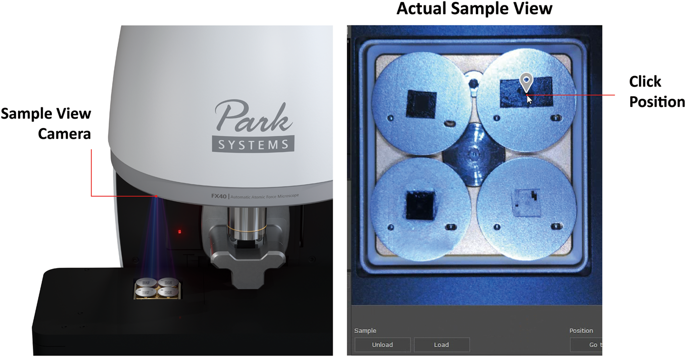
Figure 12: Sample navigation is simplified with the default off-axis sample view camera and fast moving XY stage. The picture on the left indicates the physical location of the camera, while the right picture depicts an actual screen shot of the sample stage.
Imaging
SmartScanTM is a user-friendly interface that facilitates automation of the entire imaging process and can assist in the selection of imaging parameters based on objective boundary conditions and settings. It carries out all the necessary imaging operations and intelligently selects parameters that will result in the best image quality for a given scan speed [4]. This guarantees consistent data quality, which is independent of the experience level of the operator. Processes such as cantilever frequency sweep, gain adjustment, setpoint selection, and scan speed setting are part of the automization routine [5]. Automating these processes significantly reduces the time normally taken for manual user input and trial-and-error adjustments. The images in Figure 13, which clearly reveal Moiré patterns of graphene on h-BN, typify the high-resolution results that may be obtained, independent of user experience level.

Figure 13: Moiré pattern observed on graphene on h-BN. a) Topography scan of graphene on h-BN, vertical scale 0 to 6 nm. b) Zoom in: Moiré pattern is clearly visible, vertical scale 0 to 6 nm.
After data acquisition is complete, the software secures the system by moving the Z stage upward, away from the sample, and switching the SLD off. The probe is then returned to the ATX cassette if the operator has no plans to use it immediately.
Other FX Features
There are additional groundbreaking features of the FX40 that enhance operating safety and servicing of the AFM. Multiple built-in sensors measure critical environmental conditions such as humidity, temperature, light, acoustical noise, leveling, and vibration near the system (Figure 14). The environmental conditions measured are displayed in SmartScanTM and saved with the image data file, facilitating the comparison of scanned images with various environmental conditions. Having access to these environmental indicators at any point in time may be useful to users as well as customer service engineers.
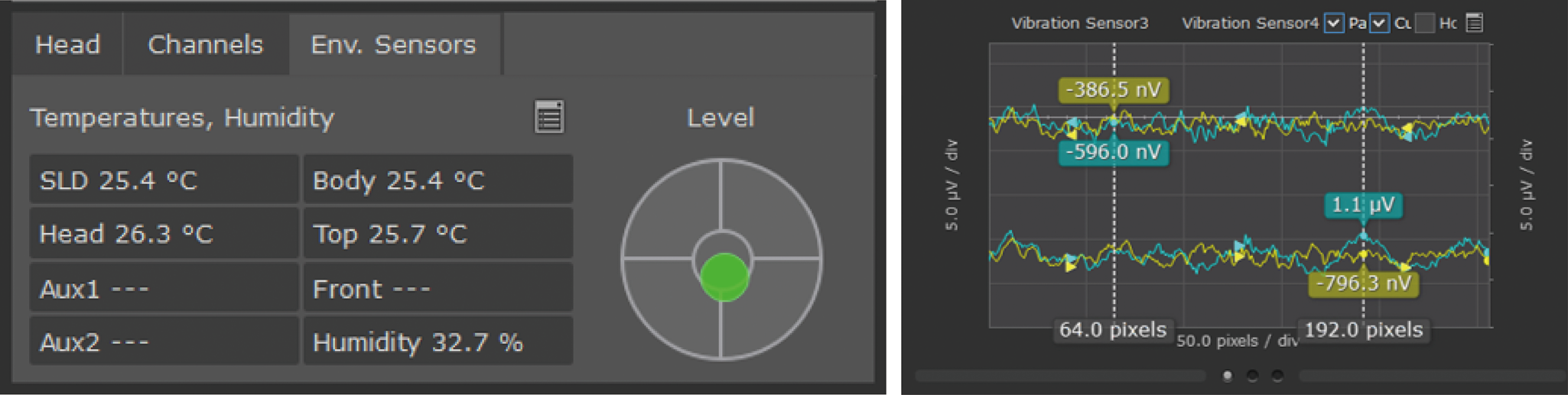
Figure 14: Various sensors monitor environmental conditions of the AFM measurement including temperature, humidity, and vibration.
Lastly, a new head crash prevention system, which uses a software interlock and hardware switch, has been developed to protect the probe and the AFM scanner from damage. A dedicated circuit monitors the SLD beam deflection and Z-detector signals in real-time, and safety intervention by an algorithmically programmed circuit ensures that the Z stage will not descend beyond the limit of a tip collision with the sample surface. This gives peace of mind to any user that their AFM system and sample are always safe from damage.
Summary
AFM is often cited as being challenging to learn and to operate by many engineers and scientists. To overcome this reputation, the FX40, a next-generation, research-grade, AFM platform has been developed with fully automated probe exchange and beam alignment that uses machine-learning technology to overcome these challenges. With simplified sample navigation and an intelligent scan algorithm, the FX40 makes enhanced performance and productivity accessible to new and experienced users alike.
Acknowledgement
The author thanks Rachel Bang for preparing the list of patents and publications, Kenneth Kang for the figures and schematics, and Dr. Sang-il Park, founder and CEO of Park Systems Corp., for his technology vision and generous comments and feedback during product development and launch preparation of the Park FX40.


