


No CrossRef data available.
Article contents
Use of surface photo-reactive nanometal printing for polymer thin-film transistors: contact resistance and short-channel effects
Published online by Cambridge University Press: 16 September 2019
Abstract
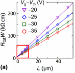
A crucial target in the printed electronics technologies is to realize all-printed thin-film transistors (TFTs), as being applicable to the industry. Here, the authors report printed polymer TFTs through the integration of the SuPR-NaP technique, a promising way for manufacturing ultrafine printed silver electrodes, with printed polymer semiconductor layers. The authors used a class of donor–acceptor-type copolymer, PDVT-10, and found that the devices exhibit excellent TFT characteristics. The devices allow the transfer length method measurements with high accuracy, where the estimated contact resistance is considerably small (4.7 kΩ cm) among the bottom-contact TFTs using printed silver electrodes, with also showing short-channel effects.
- Type
- Research Letters
- Information
- Copyright
- Copyright © Materials Research Society 2019
References
1.Sirringhaus, H.: 25th anniversary article: organic field-effect transistors: the path beyond amorphous silicon. Adv. Mater. 26, 1319 (2014).CrossRefGoogle ScholarPubMed
2.Fukuda, K. and Someya, T.: Recent progress in the development of printed thin-film transistors and circuits with high-resolution printing technology. Adv. Mater. 29, 1602736 (2016).CrossRefGoogle ScholarPubMed
3.Sekitani, T., Noguchi, Y., Zschieschang, U., Klauk, H., and Someya, T.: Organic transistors manufactured using inkjet technology with subfemtoliter accuracy. Proc. Natl. Acad. Sci. USA 105, 4976 (2008).CrossRefGoogle ScholarPubMed
4.Liu, X., Kanehara, M., Liu, C., Sakamoto, K., Yasuda, T., Takeya, J., and Minari, T.: Spontaneous patterning of high-resolution electronics via parallel vacuum ultraviolet. Adv. Mater. 28, 6568 (2016).CrossRefGoogle ScholarPubMed
5.Perinot, A., Kshirsagar, P., Malvindi, M.A., Pompa, P.P., Fiammengo, R., and Caironi, M.: Direct-written polymer field-effect transistors operating at 20 MHz. Sci. Rep. 6, 38941 (2016).CrossRefGoogle ScholarPubMed
6.Yamada, T., Fukuhara, K., Matsuoka, K., Minemawari, H., Tsutsumi, J., Fukuda, N., Aoshima, K., Arai, S., Makita, Y., Kubo, H., Enomoto, T., Togashi, T., Kurihara, M., and Hasegawa, T.: Nanoparticle chemisorption printing technique for conductive silver patterning with submicron resolution. Nat. Commun 7, 11402 (2016).CrossRefGoogle ScholarPubMed
7.Blülle, B., Häusermann, R., and Batlogg, B.: Approaching the trap-free limit in organic single-crystal field-effect transistors. Phys. Rev. Appl. 1, 034006 (2014).CrossRefGoogle Scholar
8.Kalb, W.L., Mathis, T., Haas, S., Stassen, A.F., and Batlogg, B.: Organic small molecule field-effect transistors with Cytop™ gate dielectric: eliminating gate bias stress effects. Appl. Phys. Lett. 90, 092104 (2007).CrossRefGoogle Scholar
9.Ikawa, M., Yamada, T., Matsui, H., Minemawari, H., Tsutsumi, J., Horii, Y., Chikamatsu, M., Azumi, R., Kumai, R., and Hasegawa, T.: Simple push coating of polymer thin-film transistors. Nat. Commun. 3, 1176 (2012).CrossRefGoogle ScholarPubMed
10.Kitahara, G., Aoshima, K., Tsutsumi, J., Minemawari, H., Arai, S., and Hasegawa, T.: Low-voltage operation of organic thin-film transistors based on ultrafine printed silver electrodes. Org. Electron. 50, 426–428 (2017).CrossRefGoogle Scholar
11.Aoshima, K., Arai, S., Fukuhara, K., Yamada, T., and Hasegawa, T.: Surface modification of printed silver electrodes for efficient carrier injection in organic thin-film transistors. Org. Electron. 41, 137 (2017).CrossRefGoogle Scholar
12.Chen, H., Guo, Y., Yu, G., Zhao, Y., Zhang, J., Gao, D., Liu, H., and Liu, Y.: Highly π-extended copolymers with diketopyrrolopyrrole moieties for high-performance field-effect transistors. Adv. Mater. 24, 4618 (2012).10.1002/adma.201201318CrossRefGoogle ScholarPubMed
13.Pei, K., Chen, M., Zhou, Z., Li, H., and Chan, P.K.L.: Overestimation of carrier mobility in organic thin film transistors due to unaccounted fringe currents. ACS Appl. Electron. Mater. 1, 379 (2019).CrossRefGoogle Scholar
14.Liu, J., Ge, Q., Zhang, W., Ma, J., Ding, J., Yu, G., and Hu, J.: Highly π-extended copolymer as additive-free hole-transport material for perovskite solar cells. Nano. Res. 11, 185 (2018).CrossRefGoogle Scholar
15.Uemura, T., Rolin, C., Ke, T.-H., Fesenko, P., Genoe, J., Heremans, P., and Takeya, J.: On the extraction of charge carrier mobility in high-mobility organic transistors. Adv. Mater. 28, 151 (2016).CrossRefGoogle ScholarPubMed
16.Tsutsumi, J., Matsuoka, S., Osaka, I., Kumai, R., and Hasegawa, T.: Reduced exchange narrowing caused by gate-induced charge carriers in high-mobility donor-acceptor copolymers. Phys. Rev. B 95, 115306 (2017).CrossRefGoogle Scholar
17.Kwon, S., Yu, K., Kweon, K., Kim, G., Kim, J., Kim, H., Jo, Y.R., Kim, B.J., Kim, J., Lee, S.H., and Lee, K.: Template-mediated nano-crystallite networks in semiconducting polymers. Nat. Commun. 5, 4183 (2014).CrossRefGoogle ScholarPubMed
18.Okachi, T.: Mobility overestimation due to minority carrier injection and trapping in organic field-effect transistors. Org. Electron. 57, 34 (2018).CrossRefGoogle Scholar
19.Sze, S.M.: Semiconductor Device: Physics and Technology (John Wiley & Sons, New York, NY, USA, 1985).Google Scholar
20.Haddock, J.H., Zhang, X., Zheng, S., Zhang, Q., Marder, S.R., and Kippelen, B.: A comprehensive study of short channel effects in organic field-effect transistors. Org. Electron. 7, 45 (2006).CrossRefGoogle Scholar
21.Yokota, T., Sekitani, T., Kato, Y., Kuribara, K., Zschieschang, U., Klauk, H., Yamamoto, T., Takimiya, K., Kuwabara, H., Ikeda, M., and Someya, T.: Low-voltage organic transistor with subfemtoliter inkjet source-drain contacts. MRS Commun. 1, 3 (2011).CrossRefGoogle Scholar
22.Borchert, J.W., Peng, B., Letzkus, F., Burghartz, J.N., Chan, P.K.L., Zojer, K., Ludwigs, S., and Klauk, H.: Small contact resistance and high-frequency operation of flexible low-voltage inverted coplanar organic transistors. Nat. Commun. 10, 1119 (2019).CrossRefGoogle ScholarPubMed
23.Chung, S., Jeong, J., Kim, D., Park, Y., Lee, C., and Hong, Y.: Contact resistance of inkjet-printed silver source-drain electrodes in bottom-contact OTFTs. J. Disp. Technol. 8, 48 (2012).CrossRefGoogle Scholar
24.Fukuda, K., Sekine, T., Kobayashi, Y., Kumaki, D., Itoh, M., Nagaoka, M., Toda, T., Saito, S., Kurihara, M., Sakamoto, M., and Tokito, S.: Stable organic thin-film transistors using full solution-processing and low-temperature sintering silver nanoparticle inks. Org. Electron. 13, 1660 (2012).CrossRefGoogle Scholar
25.Fukuda, K., Sekine, T., Kobayashi, Y., Takeda, Y., Shimizu, M., Yamashita, N., Kumaki, D., Itoh, M., Nagaoka, M., Toda, T., Saito, S., Kurihara, M., Sakamoto, M., and Tokito, S.: Organic integrated circuits using room-temperature sintered silver nanoparticles as printed electrodes. Org. Electron. 13, 3296 (2012).CrossRefGoogle Scholar
26.Fukuda, K., Takeda, Y., Mizukami, M., Kumaki, D., and Tokito, S.: Fully solution-processed flexible organic thin film transistor arrays with high mobility and exceptional uniformity. Sci. Rep. 4, 3947 (2014).CrossRefGoogle ScholarPubMed

Kitahara et al. supplementary material
Figure S1

Image
1.9 MB
Kitahara et al. supplementary material
Figure S2
Image
690.1 KB
Kitahara et al. supplementary material
Figure S3
Image
819.3 KB