Hostname: page-component-7479d7b7d-m9pkr Total loading time: 0 Render date: 2024-07-13T01:52:55.198Z Has data issue: false hasContentIssue false

Tin sulfide (SnS) thin-film solar cells deposited by organic chemical vapor sulfurization based on CdS and high transmittance Cd(S,O) n-type layers with the superstrate device structure

Published online by Cambridge University Press:  16 October 2020

Faruk Ballipinar*
Affiliation:
Department of Electrical and Computer Engineering, Center for Autonomous Solar Power (CASP), Binghamton University, State University of New York, Binghamton, NY13902, USA
*
Address all correspondence to Faruk Ballipinar at fballip1@binghamton.edu
Get access

Abstract

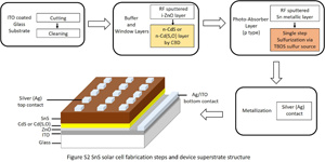
In this work, RF-sputtered metallic tin (Sn) film was sulfurized through di-tert-butyl-disulfide vapor at 350 °C for 150, 180, 210, and 240 min. According to the Raman spectra analysis, 210 min was sufficient to form dominantly SnS film. X-ray diffraction and X-ray photoelectron spectroscopy (XPS) studies of SnS film were evaluated. The n-type window layers CdS and high transmittance Cd(S,O) were deposited by chemical bath deposition through two different baths without and with TX-100 surfactant, respectively. XPS analysis of CdS and Cd(S,O) films was carried out. SnS solar cells formed in the superstrate solar cell device configuration. The photovoltaic performances were evaluated.

Type
Research Letters
Copyright
Copyright © The Author(s), 2020, published on behalf of Materials Research Society by Cambridge University Press

Access options

Get access to the full version of this content by using one of the access options below. (Log in options will check for institutional or personal access. Content may require purchase if you do not have access.)

References

Almosni, S., Delamarre, A., Jehl, Z., Suchet, D., Cojocaru, L., Giteau, M., Behaghel, B., Julian, A., Ibrahim, C., Tatry, L., Wang, H., Kubo, T., Uchida, S., Segawa, H., Miyashita, N., Tamaki, R., Shoji, Y., Yoshida, K., Ahsan, N., Watanabe, K., Inoue, T., Sugiyama, M., Nakano, Y., Hamamura, T., Toupance, T., Olivier, C., Chambon, S., Vignau, L., Geffroy, C., Cloutet, E., Hadziioannou, G., Cavassilas, N., Rale, P., Cattoni, A., Collin, S., Gibelli, F., Paire, M., Lombez, L., Aureau, D., Bouttemy, M., Etcheberry, A., Okada, Y., and Guillemoles, J.-F.: Material challenges for solar cells in the twenty-first century: directions in emerging technologies. Sci. Technol. Adv. Mat. 336369 (2018). doi:10.1080/14686996.2018.1433439.CrossRefGoogle ScholarPubMed
Zakutayev, A.: Brief review of emerging photovoltaic absorbers. Curr. Opin. Green Sustain. Chem. 4, 815 (2017).CrossRefGoogle Scholar
Burton, L.A., Colombara, D., Abellon, R.D., Grozema, F.C., Peter, L.M., Savenije, T.J., Dennler, G., and Walsh, A.: Synthesis, characterization, and electronic structure of single-crystal SnS, Sn2S3, and SnS2. Chem. Mater. 25, 49084916 (2013).CrossRefGoogle Scholar
Andrade-Arvizu, J.A., Courel-Piedrahita, M., and Vigil-Galán, O.: SnS-based thin film solar cells: perspectives over the last 25 years. J Mater. Sci.: Mater. Electron. 26, 45414556 (2015).Google Scholar
Koteeswara Reddy, N., Devika, M., and Gopal, E.S.R.: Review on tin (II) sulfide (SnS) material: synthesis, properties and applications. Crit. Rev. Solid State Mater. Sci. 40, 359398 (2015).CrossRefGoogle Scholar
Banai, R.E., Horn, M.W., and Brownson, J.R.S.: A review of tin (II) monosulfide and its potential as a photovoltaic absorber. Sol. Energy Mater. Sol. Cells 150, 112129 (2016).CrossRefGoogle Scholar
Di Mare, S., Menossi, D., Salavei, A., Artegiani, E., Piccinelli, F., Kumar, A., Mariotto, G., and Romeo, A.: SnS thin film solar cells: perspectives and limitations. Coatings 7, 34 (2017).CrossRefGoogle Scholar
Jaramillo, R., Steinmann, V., Yang, C., Hartman, K., Chakraborty, R., Poindexter, J.R., Castillo, M.L., Gordon, R., and Buonassisi, T.: Making record-efficiency SnS solar cells by thermal evaporation and atomic layer deposition. J. Vis. Exp. 99, e52705 (2015).Google Scholar
Sinsermsuksakul, P., Sun, L., Lee, S.W., Park, H.H., Kim, S.B., Yang, C., and Gordon, R.G.: Overcoming efficiency limitations of SnS-based solar cells. Adv. Energy Mater. 4, 1400496 (2014).CrossRefGoogle Scholar
Kawano, Y., Chantana, J., and Minemoto, T.: Impact of growth temperature on the properties of SnS film prepared by thermal evaporation and its photovoltaic performance. Curr. Appl. Phys. 15, 897901 (2015).CrossRefGoogle Scholar
Ballipinar, F., and Rastogi, A.C.: Single-step organic vapor phase sulfurization synthesis of p-SnS photo-absorber for graded band-gap thin film heterojunction solar cells with n-ZnO1-xSx. MRS Adv. 1, 28012806 (2016).CrossRefGoogle Scholar
Hartman, K., Johnson, L., Bertoni, M.I., Recht, D., Aziz, M.J., Scarpulla, M.A., and Buonassisi, T.: SnS thin-films by RF sputtering at room temperature. Thin Solid Films 519, 74217424 (2011).CrossRefGoogle Scholar
Xia, D.L., Xu, J., Shi, W.Q., Lei, P., and Zhao, X.J.: Synthesis and properties of SnS thin films by chemical bath deposition. Key Eng. Mater. 509, 333338 (2012).CrossRefGoogle Scholar
Ma, X., Liu, D., Yang, L., Zuo, S., and Zhou, M.: Molybdenum (Mo) back contacts for CIGS solar cells. In Eighth International Conference on Thin Film Physics and Applications, Vol. 9068, 2013; p. 906814. doi:10.1117/12.2053498.CrossRefGoogle Scholar
Ballipinar, F. and Rastogi, A.C.: High transmittance cadmium oxysulfide Cd (S,O) buffer layer grown by triton X-100 mediated chemical bath deposition for thin-film heterojunction solar cells. J. Appl. Phys. 121, 035302 (2017).CrossRefGoogle Scholar
Ballipinar, F. and Rastogi, A.C.: Tin sulfide (SnS) semiconductor photo-absorber thin films for solar cells by vapor phase sulfurization of Sn metallic layers using organic sulfur source. J. Alloys Compd. 728, 179188 (2017).CrossRefGoogle Scholar
Ballipinar, F.: Thin film solar cells based on metal sulfides and organic perovskite semiconductors. Ph.D. Dissertation, State University, New York, Binghamton, 2018.Google Scholar
Chandrashekhar, H.R., Humphreys, R.G., Zwick, U., and Cardona, M.: Infrared and Raman spectra of the IV-VI compounds SnS and SnSe. Phys. Rev. B 15, 2177 (1977).CrossRefGoogle Scholar
Nikolic, P.M., Mihajlovic, P., and Lavrencic, B.: Splitting and coupling of lattice modes in the layer compound SnS. J. Phys. C: Solid State Phys. 10, L289 (1977).CrossRefGoogle Scholar
Price, L.S., Parkin, I.P., Hardy, A.M.E., Clark, R.J.H., Hibbert, T.G., and Molloy, K.C.: Atmospheric pressure chemical vapor deposition of tin sulfides (SnS, Sn2S3, and SnS2) on glass. Chem. Mater. 11, 17921799 (1999).CrossRefGoogle Scholar
Chandrasekhar, H.R. and Mead, D.G.: Long-wavelength phonons in mixed-valence semiconductor SnIISnIVS3. Phys. Rev. B 19, 932 (1979).CrossRefGoogle Scholar
Sohila, S., Rajalakshmi, M., Ghoshc, C., Arora, A.K., and Muthamizhchelvan, C.: Optical and Raman scattering studies on SnS nanoparticles. J. Alloys Compd. 509, 58435847 (2011).CrossRefGoogle Scholar
Price, L.S., Parkin, I., Field, M.N., Hardy, A.M.E., Clark, R.J.H., Hibbert, T.G., and Molloy, K.C.: Atmospheric pressure chemical vapour deposition of tin(II) sulfide films on glass substrates from Bun3SnO2CCF3 with hydrogen sulfide. J. Mater. Chem. 10, 527530 (2000).CrossRefGoogle Scholar
Katahama, H., Nakashima, S., Mitsuishi, A., Ishigame, M., and Arashi, H.: Raman scattering study of interlayer bonding in CdI2 and SnS2 under hydrostatic pressure: analysis by use of Van Der Waals interaction. J. Phys. Chem. Solids 44, 10811087 (1983).CrossRefGoogle Scholar
Whittles, T.J., Burton, L.A., Skelton, J.M., Walsh, A., Veal, T.D., and Dhanak, V.R.: Band alignments, valence bands, and core levels in the tin sulfides SnS, SnS2, and Sn2S3: experiment and theory. Chem. Mater. 28, 37183726 (2016).CrossRefGoogle Scholar
Reddy, M.V., Babu, P., Ramakrishna Reddy, K.T., and Miles, R.W.: X-Ray photoelectron spectroscopy and X-ray diffraction studies on tin sulfide films grown by sulfurization process. J. Renew. Sustain. Energy 5, 031613 (2013).CrossRefGoogle Scholar
Zhao, L., Di, Y., Yan, C., Liu, F., Cheng, Z., Jiang, L., Hao, X., Laia, Y., and Lia, J.: In situ growth of SnS absorbing layer by reactive sputtering for thin film solar cells. RSC Adv. 6, 41084115 (2016).CrossRefGoogle Scholar
Huang, C.-C., Lin, Y.-J., Chuang, C.-Y., Liu, C.-J., and Yang, Y.-W.: Conduction-type control of SnSx films prepared by the sol–gel method for different sulfur contents. J. Alloys Compd. 553, 208211 (2013).CrossRefGoogle Scholar
Maticiuc, N., Katerski, A., Danilson, M., Krunks, M., and Hiie, J.: XPS study of OH impurity in solution processed CdS thin films. Sol. Energy Mater. Sol. Cells 160, 211216 (2017).CrossRefGoogle Scholar
Kumar, A., Kumar, V., Chandra, R., and Gautam, Y.K.: Effect of sputtering process parameters on structural and optical properties of CdS thin films. Mater. Res. Express 6, 106448 (2019).CrossRefGoogle Scholar
Supplementary material: File

Ballipinar supplementary material

Figures S1-S4 and Tables S1-S3

Download Ballipinar supplementary material(File)
File 430.8 KB