Last updated 27/06/24: Online ordering is currently unavailable due to technical issues. We apologise for any delays responding to customers while we resolve this. For further updates please visit our website: https://www.cambridge.org/news-and-insights/technical-incident
We use cookies to distinguish you from other users and to provide you with a better experience on our websites. Close this message to accept cookies or find out how to manage your cookie settings.
To save this undefined to your undefined account, please select one or more formats and confirm that you agree to abide by our usage policies. If this is the first time you used this feature, you will be asked to authorise Cambridge Core to connect with your undefined account.
Find out more about saving content to .
To save this article to your Kindle, first ensure coreplatform@cambridge.org is added to your Approved Personal Document E-mail List under your Personal Document Settings on the Manage Your Content and Devices page of your Amazon account. Then enter the ‘name’ part of your Kindle email address below.
Find out more about saving to your Kindle.
Note you can select to save to either the @free.kindle.com or @kindle.com variations. ‘@free.kindle.com’ emails are free but can only be saved to your device when it is connected to wi-fi. ‘@kindle.com’ emails can be delivered even when you are not connected to wi-fi, but note that service fees apply.
There has been increasing interest in so-called phononic materials, which can support surface modes known as surface phonon polaritons, consisting of electromagnetic waves coupled to lattice vibrations at the surface of a polar material. While such excitations have a variety of desirable features, they are limited to the spectral range between a material's longitudinal and transverse optical phonon frequencies. In this work, we demonstrate that for materials whose free-carrier concentrations can be controlled, hybrid plasmonic/phononic modes can be supported across a range of frequencies including those generally forbidden by purely phononic materials.
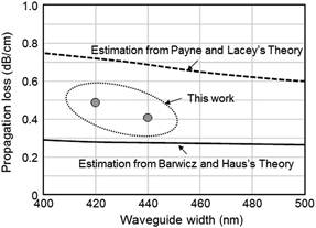
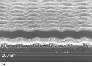
Low-propagation-loss silicon wire waveguides are key components of optical integrated circuits. In this paper, we clarified, through assessment of the relationship between waveguide loss and fabrication technology that high-resolution lithography and an adjusted lithography process window are important for low-loss waveguides. The silicon wire waveguides fabricated by high-resolution lithography technology using ArF immersion lithography process showed world-record low propagation losses of 0.40 dB/cm for the C-band and 1.28 dB/cm for the O-band. Analysis with Barwicz and Haus's theory indicated that sidewall scattering is the main cause of propagation loss even in such low-loss waveguides.
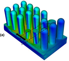
The field of nanophotonics has experienced a dramatic development in recent years, which requires ample candidate structures to achieve desirable functionalities. For many novel device designs in emerging field of transformation optics, optical metamaterials, and others, non-uniform and non-conformal thin films as well as three-dimensional (3D) structures are necessary to achieve advanced functionalities. Here, we report several techniques utilizing angled physical vapor deposition to obtain unique and complex 3D structures such as films with tapered thickness on planar substrates, tapered or uniform films on curved surfaces, and 3D nanorod arrays. These structures could enrich the existing practical design space for applications in nanophotonics and nanoelectronics.
We analyze the optical properties of composite materials that combine nanowire and nanolayer platforms. We revisit effective-medium theory (EMT) description of wire materials with high filling fraction positioned in anisotropic unit cells and present a simple numerical technique to extend Maxwell–Garnett formalism in this limit. We also demonstrate that the resulting EMT can be combined with transfer-matrix technique to adequately describe photonic band gap behavior, previously observed in epitaxially grown semiconductor multilayer nanowires.
Transparent high refractive index materials are of the central importance for the development of metasurface in visible range. Titanium dioxide (TiO2) has been considered as a perfect candidate due to its wide band gap and high refractive index. However, till now, it is still quite challenging to fabricate high-quality TiO2 films with high refractive indices and low losses. Here we demonstrate the fabrication of high-quality TiO2 film using an electron-beam evaporation method. We show that the post-annealing conditions play key roles in the microstructure crystallographic and the optical refractive index of the TiO2 films. A predominately oriented TiO2 film has been achieved by annealing at 700 °C in oxygen ambient. The refractive index is as high as 2.4, and the corresponding loss is negligible at 632 nm. Further studies on dielectric antennas show that our TiO2 film can be an ideal platform to fabricate metasurface in visible frequency range. We believe that our research will be important for the advances of all-dielectric metasurfaces.
Plasmonics, Photonics, and Metamaterials Prospective Article
We propose a surface integral equation simulation scheme which incorporates the integral equation fast Fourier transform accelerative algorithm and domain decomposition method. Such scheme provides efficient and accurate solutions for substrate-supported non-periodic plasmonic array platforms with large number of building blocks and complex element geometry. The effect of array defects can be systematically and successfully studied taking advantage of the considerable flexibility of the domain decomposition approach. The proposed model will be of great advantage for fast and accurate characterization of graded-pattern plasmonic materials and metasurfaces.
Plasmonics, Photonics, and Metamaterials Research Letter
We present two straightforward and cost-effective methods, based on metal-assisted chemical etching and a direct imprinting technique, to fabricate metal-covered porous amorphous silicon back reflectors for amorphous silicon solar cells. We demonstrate an increase of approximately 30% in both short-circuit current and overall efficiency with respect to a cell with a flat metal back reflector. This is achieved by implementing light trapping via either a roughened porous amorphous silicon layer or an imprinted periodic grating. This work provides a pathway to increase amorphous silicon solar cell efficiency via increased absorption without significantly impacting processing costs.
Plasmonics, Photonics, and Metamaterials Prospective Article
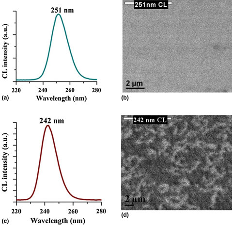
This paper reviews progress in ultraviolet (UV) optoelectronic devices based on AlGaN films and their quantum wells (QWs), grown by plasma-assisted molecular beam epitaxy. A growth mode, leading to band-structure potential fluctuations and resulting in AlGaN multiple QWs with internal quantum efficiency as high as 68%, is discussed. Atomic ordering in these alloys, which is different from that observed in traditional III–V alloys, and its effect on device performance is also addressed. Finally, progress in UV-light-emitting diodes, UV lasers, UV detectors, electroabsorption modulators, and distributed Bragg reflectors is presented.
Plasmonics, Photonics, and Metamaterials Research Letters
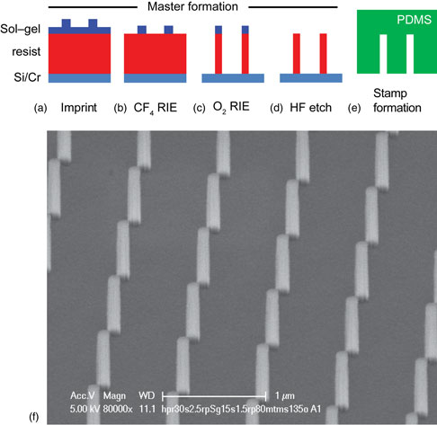
We present a novel soft-nanoimprint procedure to fabricate high-quality sub-wavelength hole arrays in optically thick films of gold on glass substrates. We fabricate 0.5 × 0.5 mm2 structures composed of a square array of 180 nm-diameter holes with a 780 nm pitch. Optical angular transmission measurements on the arrays show clear extraordinary transmission peaks corresponding to the dispersion of surface plasmon polaritons propagating on either side of the metal film. The transmission features can be strongly controlled by engineering the dielectric environment around the holes. As the nanoimprint procedure enables fabrication of nanoscale patterns over wafer-scale areas at low cost, these imprinted metal nanoparticle arrays can find applications in, e.g., optical components, photovoltaics, integrated optics, and microfluidics.
Plasmonics, Photonics, and Metamaterials Prospective Article
Photonic crystal nanolasers are fabricated and operated simply, and can be applied as disposable sensors for biomedical applications. They are sensitive to the change with environmental index and surface charge. Functionalizing the nanolaser surface with an antibody, the specific binding of target antigen is detected with a detection limit 2–4 orders lower than that achieved by current standard methods, enzyme-linked immuno-sorbent assay. Nanolasers also detect negatively-charged deoxyribonucleic acid from their emission intensity. This technique requires neither labels nor spectroscopy, which simplifies screening procedures. Its applicability for high-speed detection of endotoxin and for label-fee imaging of living cells are also demonstrated.
Plasmonics, Photonics, and Metamaterials Research Letters
Metatronics, or metamaterial-inspired optical nanocircuitry, has provided a powerful toolset to tailor and implement modular quasi-static circuit functionalities in the optical regime. So far, these concepts have been mostly limited to linear operations, while many of the relevant operations in integrated circuits require nonlinear responses. In this work, we introduce nonlinear infrared nanocircuit elements exploiting large quantum conductance driven by photon-assisted tunneling and enhanced by hybrid plasmonic nanojunctions. Based on these concepts, we present infrared lumped nanocircuit mixers and switches for second-harmonic generation, and wide-spectrum self-amplitude modulators based on nanorods.
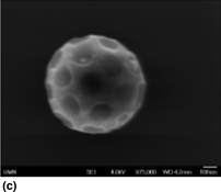
In this work, photonic crystals of plasmonic/excitonic semiconductor nanocrystals (NCs) were assembled from non-thermal plasma-synthesized boron (B)-doped silicon (Si) NCs. The photonic crystals form an inverse opal structure with larger refractive index than the conventional crystals made from silica nanoparticles and are aimed at controlling light propagation via excitonic and plasmonic absorption of the B-doped Si NC as well as the photonic band gap of the photonic crystal. Furthermore, we demonstrate self-assembly of mesoscopic photonic crystal particles consisting of B-doped Si NCs with well-defined inverse opal structure via simple aerosol processing.
Optoplasmonic networks consisting of dielectric microsphere resonators and plasmonic nanoantennas in a morphologically well-defined on-chip platform support unique electromagnetic signatures that are hybrids of photonic whispering gallery modes and localized surface plasmon resonances. Here we explore the dependence of their near- and far-field responses on the key structural parameters, including the size of the gold nanoparticles forming the plasmonic elements, the separation between the microspheres, and the geometry of the chain. The high degree of structural flexibility, which is experimentally accessible through template guided self-assembly approaches, makes these optoplasmonic structures a unique electromagnetic material for tuning spectral shapes and intensities.
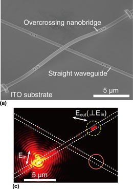
Plasmonic waveguides can transport light while still confining it beyond the diffraction limit. Recently, crossing plasmonic waveguides have been suggested for the implementation of higher-density optical networks. However, suppressing undesirable scattering at their crossing point is still a challenging task because waveguides in these structures are physically connected. Here, we present an experimental demonstration of surface plasmon propagation on an overcrossing metallic waveguide fabricated by a pick-and-place method. By spatially separating the waveguides, the undesirable interaction at the interconnection can be suppressed. Our approach could be a powerful platform to achieve high-density integration of optical waveguides.