Introduction
Cloud computing (CC) is a computational paradigm that delivers on-demand computing resources, everything from customized applications to data centers, over the internet. This paradigm has several advantages over the traditional on-premise approach, including dynamically scalable, virtualized computing resources and the economics of scale. However, the technologies involved are modern and complex, and in general the frameworks to enable these technologies are not familiar to electron microscopists.
Computer simulation plays a critical role in electron microscopy as it does in every other scientific branch, from education to research and applications. The theories behind electron microscopy are broad, ranging from crystallography to optics, and from classical mechanics to quantum physics. How to teach these broad concepts to students and how to relate theory with practice are the challenges faced by every instructor of electron microscopy. How to teach complicated concepts, such as aberration correction, with limited access to instrument resources is also a challenge. Computer simulations in principle can bridge these gaps. However, the capability and availability of electron microscopy simulation tools are both limited.
Methods for electron microscopy simulations are also widely used in quantifying electron images and diffraction patterns, producing applications that require a great amount of computational resources. Such resources are currently available only to limited institutes worldwide. CC thus could enable the sharing of such resources among the microscopy community, as well as provide the infrastructure support for implementing high-performance computing algorithms.
Here, we explore the CC for electron microscopy using cloudEMAPS, which is designed to demonstrate the feasibility of CC for both microscopy research and teaching. In what follows, we will review the current practices and the implementation of CC as a platform to further microscopy-related materials and biological research, as well as providing the basic utilities to serve the microscopy community.
Current Practices
There have been many past attempts at building simulation tools for microscopy education and research, including JEMS (a Java-based electron microscopy software), various multislice simulation codes, and an early Macintosh computer-based software (IdealMicroscope) for electron diffraction simulation. These software products were developed as desktop applications, using the limited access model, and they are generally not available as broadly based education and research tools. The exception is webEMAPS for web-based electron microscopy application software [Reference Zuo and Mabon1], which had successes in offering electron diffraction simulation to the broad community via the internet. However, webEMAPS was hosted on a single computer running the Microsoft server 2000. Even though webEMAPS performed remarkably well as an internet accessible solution over a ten-year period here at the University of Illinois and attracted many users across the world, it lacked scalability as well as upgradability. Most critically, it lacked the internet security required to meet today's digital enterprise and privacy requirements. For this reason, the site was shut down by the University.
Remarkable advances in CC have been made over the past decade, with competing cloud services emerging from major technological companies, as well as research institutions. However, current adaptations of the CC environment for science and engineering are built with considerable resources and institutional support. For example, the NSF-supported nanoHUB runs via a distributed computing network at Purdue University, as well as the TeraGrid and Open Science Grid [Reference Klimeck2]. The Materials Project computes properties of all known crystals, which is hosted on supercomputing clusters at national laboratories that enable the underlying computations, data retrieval, and algorithms to run at fast speeds [Reference Jain3]. For data archiving and retrieval, the resources required are modest. Such resources are offered, for example, by nanoHUB, which includes lectures and notes in electron microscopy, the DigitalMicrograph database hosted at the Austrian Center for Electron Microscopy and Nanoanalysis, and the EELS data base at https://eelsdb.eu.
Implementation of cloudEMAPS
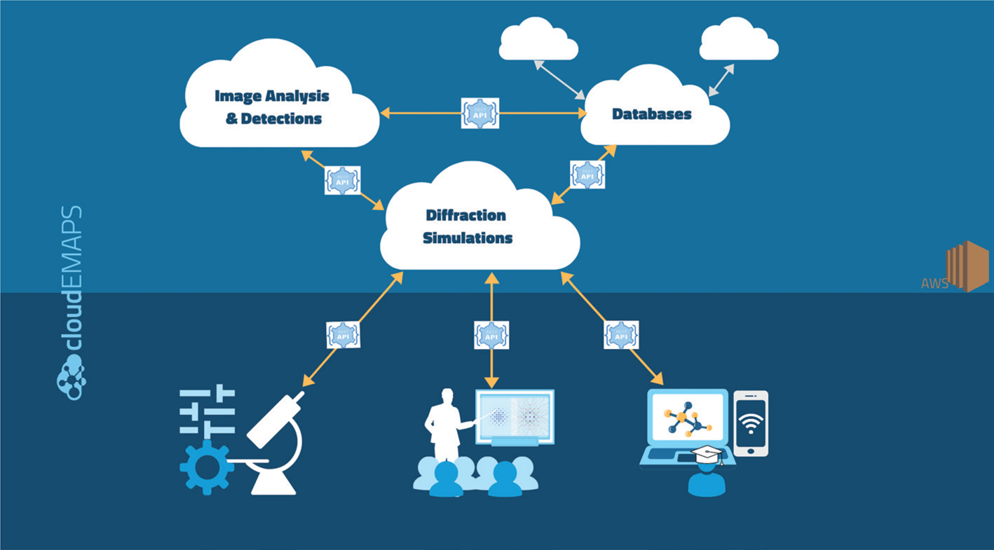
We use Amazon Web Service (AWS) for CC, which is broadly available at a relatively low cost and is secure. Figure 1 illustrates how electron microscopy simulation works in cloudEMAPS. On the client side, users run a browser-based graphics user interface (GUI) using a portable device or a desktop computer. Upon user input, the frontend browser sends an HTTP request to the cloud server, which contains the data on the user's side as a payload. The payload includes the microscope control settings and sample information such as crystal data and zone axis orientation. Once the payload is received, the server parses and validates the request, allocates necessary computing resources, and executes the corresponding computation. When the computation finishes, the server parses and elicits a response with the results in a return payload formatted in JSON (JavaScript Object Notation) for the frontend web browser to render in a graphical canvas. This way the end-user can observe in real time the result of their operation and simulate the microscope operation.

Figure 1: Schematic workflow of cloudEMAPS. The CC part is connected to user devices through RESTful communication protocols, while the web browser provides the user interfaces.
The electron microscopy computations are performed in the backend on the cloud. The computations currently include electron diffraction pattern and image simulations using a defined crystal model and simulation of aberration-corrected electron optics. These applications require a few input data and computational steps that range from being relatively simple, as in the case of kinematical diffraction simulation, to relatively complex in the case of dynamical convergent beam electron diffraction simulations. The output data that come back from the simulations is also relatively small in the form of an image or descriptive data about diffracted beam positions and intensity.
The overall design is comprised of three parts, backend, frontend, and communication and web security. Each part is described in more detail below.
Backend
This is where all cloudEMAPS computations are located. The requests from frontend are passed to and translated into commands to cloudEMAPS‘s computing core, which, in turn, send back the computing results to the user's browser for more processing and eventually visualization. The computation is done using the LINUX-based computer programs, QED (Quantitative Electron Diffraction), BLOCH (Bloch wave method), MXTAL (Maker of Crystal models), and Probe (for aberration-corrected probe, contrast transfer, Ronchigram, and high-resolution electron microscopy simulations). Each program runs on the command-based inputs. The principles behind these computer programs are described in several books [Reference Spence and Zuo4–Reference Zuo and Spence6].
Frontend
An Internet browser is used as the frontend for user input and display of returned computational results. Figure 2 shows the major parts of the user interface displayed on a web browser. The web page contents are dynamically generated using HTML (Hyper Text and Meta Language), CSS (Cascading Style Sheet), and JavaScript, which communicates with the backend by HTTP transport. The frontend is interactive, as users can change the microscope and diffraction control parameters and have results displayed in real time.

Figure 2: cloudEMAPS user interface and display window. Interactive controls are designed to simulate transmission electrion microscopy operations.
Communication and web security
We use Nginx API management module [7] to provide the following security and performance benefits for the backend: 1) authentication and authorization and 2) rate limiting. Authentication and authorization create and manage API keys; validate JWT (JSON Web Token) to authenticate API consumers, such as the frontend, shared keys with API consumers; and import API keys from external systems [8]. Rate limiting mitigates common attacks, such as DDoS attacks and protects backend computing and database cores. This also enforces varying rate limits based on frontend API needs.
RESTful APIs are used as an application program interface that uses HTTP requests to GET, PUT, POST, and DELETE data [Reference Chen9]. cloudEMAPS uses the REST APIs’ server-client based, stateless network protocols to communicate the user's changes in microscope and other control parameters as RESTful requests to the backend and to send the backend computing results and representation back to the user's client for simulation rendering.
Application Examples
With the above infrastructure in place, we developed the following applications to demonstrate the utility of CC for electron microscopy.
Kinematical diffraction simulation
Interactive diffraction pattern simulation is provided using controls that simulate crystal tilts and diffraction deflection. An example is provided in Figure 3, where a GaAs crystal is tilted off the [Reference Zuo and Mabon001] zone axis using Tilt-X and Tilt-Y in the control panel. The camera length and detector size are separated as specified under “Microscope.” The position of a diffracted beam is determined by Bragg's law, while we use the line equation methods described to simulate Kikuchi lines [Reference Spence and Zuo4]. To run a diffraction simulation, a crystal dataset is selected and loaded first using the methods described in Figure 2. A set of crystal data can be pre-defined or user-modified for custom simulations. Enhancement in data sharing will be introduced in the future for users to share their created crystal data. The crystal data are displayed in a control panel, which contains the unit cell dimensions, atomic positions, symmetry, and the starting zone axis. HOLZ (high order Laue zone) lines are simulated in the CBED (convergent beam electron diffraction) mode. The major applications of kinematical diffraction simulation include crystal orientation determination, diffraction pattern indexing, phase identification, and reciprocal space navigation.

Figure 3: An example of kinematical diffraction pattern simulation.
Bloch wave dynamical simulation
This tool calculates the dynamical electron diffraction intensity using the Bloch wave method [Reference Zuo10]. For a small unit cell crystal, the simulation is fast enough so interactive dynamical diffraction simulation can be performed. The sample thickness can also be varied interactively. The current version calculates a diffraction pattern on a detector of 512 × 512 pixels and the number of sampling points within a CBED disk according to (CBED disk size) / 0.02. Figure 4 shows examples of the simulated CBED patterns for different crystals. The major applications of such simulations include crystal thickness determination, phase identification, and symmetry determination.

Figure 4: Bloch wave diffraction simulations on example crystals with the specified sample thickness.
For a large unit cell crystal, Bloch dynamical simulation calculation requires extensive computing power. Here, CC could provide the cutting-edge computer power to enable such calculations in a relatively short time. In the future, we plan to explore parallel computing to further reduce the computational time.
Aberration-corrected electron optical simulation tool
Understanding how different aberrations impact on electron optical performance is the essential part of aberration-corrected electron microscopy. This tool currently provides electron probe, contrast transfer function (CTF), and Ronchigram simulation capabilities. Aberrations up to 5th order are included, which can be changed separately. Figure 5 shows examples as well as the control panel for objective lens aberrations.

Figure 5: From left to right: simulated electron probe, Ronchigram, and CTF using the measured aberration coefficients from a JEOL 2200 aberration-corrected S/TEM.
Conclusions
We have demonstrated the utility and protocols of CC for electron microscopy applications. The cloud and web programming technologies employed provide a clear path for creating future innovative solutions for microscopy-related computing and simulations, and scientific computing in general. The demonstrated interactive features are expected to greatly benefit microscopy education and training. Future plans to expand upon the initial success for advanced computation are also discussed. With the CC platform in place, we welcome collaborations to accelerate scientific innovations in microscopy computation [11].
Acknowledgements
We would like to thank our current and past users of cloudEMAPS for their valuable comments and feedback. We also thank Dr. James Mabon of University of Illinois for stimulating discussions and the City of Champaign, IL, for a seed funding grant to start this project.


