


Introduction
The fractal antenna has emerged as a new area of study for advanced electronics and wave propagation research in recent years [Reference Bharti, Bharti and Sivia1]. Due to repeating identical patterns, fractal antennae essentially have multiband properties [Reference Singhal and Singh2]. The industry transitioned from traditional wideband antennae to advanced antennae [Reference Kumar and Pharwaha3]. Antennae are inexpensive and may be used for wideband applications, and because of their fractal design, they can be used for several bands and various applications [Reference Karthikeya, Abegaonkar and Koul4–Reference Ali, Subhash and Biradar6]. As multiband technology advances, antennae can now accommodate more applications in various bandwidths throughout a broader spectrum and reject signals that fall outside their frequency range [Reference Ali, Subhash and Biradar6–Reference Kumar and Singh9]. The industry demands a low-profile and compact-sized antenna that can be fabricated easily. During the last few years, researchers have been working toward minimizing the size of antennae that cover a more comprehensive range of applications [Reference Kumar and Singh9–Reference Garg, Nair, Singhal and Tomar11]. Due to fractal shape slots, a microstrip patch antenna has high gain and follows multiband characteristics, by which an antenna covers various applications.
In order to study the literature survey, Bharti et al. [Reference Bharti, Bharti and Sivia1] presented “a multiband nested square-shaped ring fractal antenna design with circular ring elements for wireless applications,” demonstrating its suitability for multiple frequency bands. Kumar and Pharwaha [Reference Kumar and Pharwaha3] developed “a modified Hilbert curve fractal antenna optimized for multiband applications.” Singh and Singh [Reference Singhal and Singh2] introduced “an elliptical monopole-based super wideband fractal antenna,” expanding the possibilities for wideband communication.
Karthikeya et al. [Reference Karthikeya, Abegaonkar and Koul4] proposed “a low-cost, high-gain triple-band mmWave Sierpinski antenna loaded with uniplanar Electromagnetic Band Gap (EBG) for 5G applications.” Singh and Singh [Reference Singh and Singh5] focused on designing and optimizing “a modified Sierpinski fractal antenna, emphasizing its potential for broadband applications.” Ali et al. [Reference Ali, Subhash and Biradar6] contributed “a miniaturized decagonal Sierpinski ultra wide band (UWB) fractal antenna suitable for ultra-wideband applications” [Reference Ali, Subhash and Biradar6].
Choukiker and Behera [Reference Choukiker and Behera7] introduced “a wideband frequency-reconfigurable Koch snowflake fractal antenna,” enabling adaptability across different frequency ranges. Ullah and Tahir [Reference Ullah and Tahir12] proposed “a novel snowflake fractal antenna for dual-beam applications in the 28 GHz band,” emphasizing its suitability for modern communication systems.
Bhatia and Sivia [Reference Bhatia and Sivia13] explored the design of “fractal antenna arrays for multiband applications,” highlighting the potential benefits of array configurations in enhancing antenna performance. Sran and Sivia [Reference Sran and Sivia14] presented “an artificial neural network (ANN) and iterated function system (IFS) based wearable hybrid fractal antenna with DGS for S, C, and X-band applications,” showcasing the role of computational intelligence in antenna design.
Several review articles have provided comprehensive overviews of fractal antennae and their applications. Praveena and Ponnapalli [Reference Praveena and Ponnapalli8] offered “a review of the design aspects of fractal antenna arrays,” summarizing the key research trends in this field. Rani [Reference Rani15] provided a comprehensive review of “various fractal antenna geometries in wireless communication,” while Aravindraj et al. [Reference Aravindraj, Nagarajan and Kumaran16] discussed the “design and analysis of recursive square fractal antennas for WLAN applications.”
The integration of metamaterials and resonators with fractal antennae has also been explored. Ahmad and Nornikman [Reference Ahmad and Nornikman17] introduced “a fractal microstrip antenna with Minkowski Island split ring resonators for broadband applications.” Sharma et al. [Reference Sharma, Lakwar and Garg18] designed a multiband low-cost fractal antenna based on parasitic split ring resonators, showcasing fractal geometries and metamaterial concepts.
Dangkham and Phongcharoenpanich [Reference Dangkham and Phongcharoenpanich19] developed “a compact split ring resonator antenna for UHF-RFID passive tags, addressing the requirements of the Internet of Things (IoT) and RFID applications.”
Additional innovations include the work of Sivia et al. [Reference Sivia, Singh and Kamal20], who employed “artificial neural networks to design a Sierpinski carpet fractal antenna,” and the research by Singhal [Reference Singhal21], who proposed “a four-arm windmill-shaped super wideband terahertz MIMO fractal antenna.”
Recent research by Raj and Mandal [Reference Raj, Dhubkarya, Srivastava and Mandal22] introduced “a high-gain Sierpinski carpet fractal antenna with square-shaped slot cuts for wireless applications,” highlighting its potential in emerging communication systems. Moreover, fractal antennae have emerged as promising candidates for various wireless applications due to their compact size and wideband characteristics. Researchers have explored various fractal geometries, design techniques, and integration with metamaterials and resonators to enhance their performance and adaptability. These advancements pave the way for the development of advanced antenna systems to meet the demands of modern wireless communication technologies.
The radiation pattern is broad when using a single antenna [Reference Quintero, Zurcher and Skrivervik23], but the gain is low. However, the gain and other properties are improved when using a single-element antenna in an array design [Reference Kumar, Kumar, Ali, Kumar and Sb24–Reference Kumar, Ali and Kumar26]. Fractal-inspired array antennae exhibit promising adaptability and scalability for future wireless communication technologies beyond 5G and 6G. Their inherent self-similarity properties allow for versatile tuning across frequency bands, making modifications relatively feasible. By adjusting the fractal geometry, these antennae can efficiently accommodate emerging frequency bands and evolving communication standards [Reference Rao, Madhav, Anilkumar and Nadh27, Reference Raj and Mandal28, Reference Rahimi, Maleki, Soltani, Arezomand and Zarrabi29, Reference Dastranj, Ranjbar and Bornapour30, Reference Kaur and Sivia31, Reference Pandeeswari and Raghavan32].
However, ensuring optimal performance may require sophisticated design and optimization processes, leveraging advanced computational tools to tailor antenna characteristics to the specific requirements of each new wireless standard. Moreover, while fractal-inspired antennae offer adaptability, fine-tuning for upcoming technologies necessitates careful engineering efforts.
However, array antennae A, B, C, and D are formed by taking elements a, b, and c. Array [A] started out with element antenna (a), and then scaled down by 50% to design array [B]. Similarly, arrays [C] and [D] were scaled down by 50% and 75% with respect to B (c) and C (a, c), respectively. The maximum return loss of 37, 32.8, 31.2, and 23 dB is described as a more radiating antenna for designs A, B, C, and D.
Furthermore, the bandwidths allocated to applications within the 5G NR and sub-6G frequency ranges of 20.88–22.8, 23.3–24.03, 26.7–27.4, 27.6–30, 30.2–31.5, 33.3–38.6, 378.7–39.96 GHz, and 22.5–25.9, 27–30.7, 31.25–33.92, 34.8–39.45 GHz, and 26–28, 32–35.5, 37.7–39.27 GHz, and 26–28.5, 34.3–35.8, 38.26–39.26 GHz, are 1.92, 0.73, 0.7, 2.4, 1.3, 5.3, and 1.26 GHz, and 3.4, 3.7, 2.67, 4.65 GHz, and 2, 3.5, 1.57 GHz, and 2.5, 1.5, 1.0 GHz with respect to designs A, B, C, and D.
The suggested antennae, designed with multiband capabilities, cater to diverse applications across 5G NR bands (n257, n258, n259, n260, and n261) and sub-6G bands, including ground-based radio navigation. Developed through CST, these antennae were successfully tested using VNA, spectrum analyzer, and power sensor.
Antenna design
Microstrip patch antenna design parameters are determined using specified mathematical formulas [Reference Sivia, Singh and Kamal20]. Deriving effective dielectric constant (εreff) involves calculations, as discussed by [Reference Sivia, Singh and Kamal20] in considering the composite material’s electrical properties:
 \begin{equation}{\text{W = }}\frac{1}{{2{\text{fr}}\sqrt {\mu \varepsilon } }}\,\sqrt {\frac{2}{{\epsilon r + 1}}} \end{equation}
 \begin{equation}{\varepsilon _{_{{\text{reff}}}}} = \frac{{\epsilon r + 1}}{2} + \frac{{\varepsilon r - 1}}{2}{\left( {1 + 12\frac{h}{w}} \right)^{\frac{{ - 1}}{2}}}\end{equation}
 where h is the height of dielectric substrate in mm, w is the width of patch, and  ${{\boldsymbol{\varepsilon }}_{\text{r}}}$ is the dielectric constant.
Once W is found using equation (2), determine the extension of length as follows:
 \begin{equation}\Delta L = h\frac{{\left( {{ }{\boldsymbol{\varepsilon }}{\text{reff }} + 0.3} \right)\left( {\frac{{W\,}}{h} + 0.264} \right)}}{{\left( {{ }{\boldsymbol{\varepsilon }}{\text{reff }} - 0.258} \right)\left( {\frac{{W\,}}{h} + 0.8} \right)}}\end{equation}
The actual length of patch is
 \begin{equation}{\text{L}} = (\frac{1}{{2fr\sqrt {\varepsilon \,\,} }} \times \frac{1}{{\sqrt {\mu \varepsilon } }}) - 2\Delta L\end{equation}
Effective length, L1 = L + 6 h, effective width W1 = W + 6 h, and
 \begin{equation}{\text{Band width \% }} = \frac{{2\left( {f2 - f1} \right)}}{{f1 + f2}}\,*{\text{ }}100\end{equation}
The feed point position for 50 Ω can be calculated as follows:
 \begin{equation}{{\text{Z}}_{{\text{in}}}}{\text{ = 1/}}{{\text{Y}}_{{\text{in}}}}{\text{ = }}{{\text{R}}_{{\text{in}}}}{\text{ = 1/2}}{{\text{G}}_{\text{1}}}\end{equation}
where Rin(y = y0) is 50 Ω and Rin(y = 0) is roughly given as follows:
 \begin{equation*}{{\text{Z}}_{{\text{in}}}}{\text{ = 1/}}{{\text{Y}}_{{\text{in}}}}{\text{ = }}{{\text{R}}_{{\text{in}}}}{\text{ = 1/2}}{{\text{G}}_{\text{1}}}\end{equation*}
 \begin{equation}{{\text{G}}_{\text{1}}}{\text{ = }}\left\{ {\begin{array}{*{20}{c}}
{\frac{1}{{90}}{{\left( {\frac{W}{\lambda }} \right)}^2}\,\,\,\,\,\,\,\,\,\,\,\,\,\,\,\,\,\,\,\,\,\,W \ll \lambda \,\,\,} \\
{\frac{1}{{120}}\left( {\frac{W}{\lambda }} \right)\,\,\,\,\,\,\,\,\,\,\,\,\,\,\,\,\,\,\,\,\,W \gg \lambda \,\,\,\,\,\,\,\,}
\end{array}} \right.\end{equation}
\begin{equation}{{\text{G}}_{\text{1}}}{\text{ = }}\left\{ {\begin{array}{*{20}{c}}
{\frac{1}{{90}}{{\left( {\frac{W}{\lambda }} \right)}^2}\,\,\,\,\,\,\,\,\,\,\,\,\,\,\,\,\,\,\,\,\,\,W \ll \lambda \,\,\,} \\
{\frac{1}{{120}}\left( {\frac{W}{\lambda }} \right)\,\,\,\,\,\,\,\,\,\,\,\,\,\,\,\,\,\,\,\,\,W \gg \lambda \,\,\,\,\,\,\,\,}
\end{array}} \right.\end{equation}Design and simulation
Simulation and analysis of element antennae
Figure 1 and Table 2 present the utilization of an Fr4 substrate measuring 1.6 mm in height, 10 mm in length, and 10 mm in width for antenna a. Subsequently, antennae b and c showcase the creation of these elements with a patch height of 0.75 mm, incorporating square and circular slots. As indicated in Table 2, the line feed uses a feeding approach with a width of 2 mm and a length of 5 mm. Demonstrating wide bandwidth and a pronounced wide band notch, Fig. 2 and Table 3 highlight the maximum return loss at 34, 42, and 50 dB for antennae a, b, and c, respectively, alongside a broad band with a reference line of 10 dB. Table 3 details various parameters for antennae a, b, and c.

Figure 1. Element antennae a, b, and c for concerning arrays.

Figure 2. Element antennae a, b, and c with some fractal fragments in the range of 20–40 GHz.
Efficient equivalent network for antenna impedance matching
The fractal-inspired design in the proposed array antennae significantly enhances their wideband performance. Incorporating fractal slots in each element antenna improves the gain and radiation pattern compared to a single antenna. This design approach, coupled with a hybrid feed and specific dimensions, results in wide bandwidth at resonating notches. The proposed antenna’s equivalent circuit modeling relies on fundamental principles of electrical engineering and antenna design rooted in the theory of transmission lines. We achieve efficient power transfer from the 50 Ω source impedance (ZS) to the antenna (ZL) by treating the antenna as a transmission line. This approach aligns source and load impedances, reducing signal reflections and losses, a well-established RF and antenna engineering practice to optimize performance. Moreover, we incorporate T and Pi networks to model the 5 mm feedline separately. Its ability to account for complex impedance transformations and transmission line losses justifies this step. These networks (Fig. 3) accurately depict the feedline’s impedance characteristics, which is critical for maintaining desired impedance matching across the entire antenna system.

Figure 3. Schematic representation of the proposed antenna’s efficient equivalent network model.

Figure 4. Array antennae A, B, C, and D with some fractal fragments through scaling down with 43%,43%, and 89%, in range of 20–40 GHz.
Simulation and analysis of array antennae with element antenna a, b, and c
As shown in Fig. 5 and Tables 1 and 2, the dimensions (width × length) of the ground of the concerning designs, A, B, C, and D, are 100 × 100 mm2, 50 × 50 mm2, 25 × 25 mm2, and 18.75 × 18.75 mm2, respectively. Here is the first step, an array [A] is formed with the help of a simple element patch (a) with presented notations in Table 2 and Fig. 5. Here total 16 number of elements antenna are formed with hybrid feed with matched 50 ohms’ connector.

Figure 5. Array antennae A, B, C, and D with some fractal fragments through scaling down, in range of 20–40 GHz.
Table 1. Design parameters for array antennae A, B, C, and D

Table 2. Notations and dimension of design parameters for designs a, b, c, A, B, C, and D

A hybrid feed optimizes antenna performance by precisely controlling signal phase and amplitude in each element and enables superior beamforming, enhancing signal strength and coverage. It offers design flexibility, integrating elements and signal processing for tailored system solutions, yielding higher gain and directivity than traditional feeds. Array antennae A, B, C, and D are formed by taking elements a, b, and c. Initially, array [A] is designed with an element antenna (a); before going to the exact scaling factor, first go through various scaling factors, as mentioned about 43% and 89%, and analyze various parameters, so resonance and impedance matching are not satisfactory with the corresponding required applications and reflection coefficient plot shown in Fig. 4, so further scaling is going through the reduction of the size by a scaling factor of 50% and the formation of array [B]. For arrays [C] and [D], scaling down by 50% and 75% concerning B(c) and C(a, c) achieved a satisfactory result with good impedance matching concerning multiple resonance.
Table 3. Comparative study with different parameters of design a, b, and c

The antenna array formation involves 16 elements (c), (a, c), and (b, c) with a 0.75 mm height, configured with hybrid excitation and matched 50-ohm connectors [B], [C], and [D]. Circular and square slots, meeting fractal requirements, are incorporated for miniaturization, ensuring wide and multiband functionality with resonating frequencies below 6 GHz and in 5G bands. This modification reduces the patch area. Figures 4 and 5 display S11 results for array antennae A, B, C, and D, indicating maximum return losses of 37, 32.8, 31.2, and 23 dB. The enhanced design of antennae B, C, and D is emphasized by these greater return losses compared to design.
Furthermore, Table 4 reveals the bandwidths for applications which operate within the 5G NR and sub-6G frequency ranges of 20.88–22.8, 23.3–24.03, 26.7–27.4, 27.6–30, 30.2–31.5, 33.3–38.6, 378.7–39.96 in GHz; and 22.5–25.9, 27–30.7, 31.25–33.92, 34.8–39.45 in GHz; and 26–28, 32–35.5, 37.7–39.27 in GHz, and 26–28.5, 34.3–35.8, 38.26–39.26 in GHz are reveals such as 1.92, 0.73, 0.7, 2.4, 1.3, 5.3, and 1.26 in GHz; and 3.4, 3.7, 2.67, 4.65 in GHz; and 2, 3.5, 1.57 in GHz; and 2.5, 1.5, 1 in GHz concerning designs A, B, and D.
Table 4. Comparative study with different parameters of array A, B, C, and D

The proposed antennae, encompassing designs A, B, C, and D, feature multiband and multi notches at frequencies including 21.5, 23.8, 27.1, 29, 30.4, 33.66, 37.1, 39.08, 25.35, 27.6, 29.2, 29.25, 32, 35, 37.5, 39.2, 27.32, 33, 37.86, 27.6, 35.36, and 38.86 GHz. This configuration extends application coverage to n257, n258, n259, n260, and n261 5G NR bands and sub-6G bands, including ground-based radio navigation applications.
Return loss (S11) and voltage standing wave ratio
Figures 6 and 7 and Table 5 represent the voltage standing wave ratio (VSWR) value as 1.02, 1.16, 1.06, 1.1, 1.18, 1.16, 1.10, and 1.07, and 1.10, 1.048, 1.07, and 1.055, and 1.18, 1.05, and 1.6, and 1.55, 1.2, and 1.23, which are in the range of 0–2, for concerning antennae A, B, C, and D. As the VSWR values are near 1, it depicts a good impedance matching. Moreover, array-level matching involves ensuring consistent impedance characteristics across all elements in the array. This helps maintain a uniform current distribution and radiation pattern across the array, minimizing mismatch losses and maintaining good VSWR performance. Equations 8 and 9 express the reflection coefficient and return loss, determined through VSWR values, aiding in the comprehension of simulated and experimental outcomes.

Figure 6. S11, VSWR, vs frequency graph for proposed antennae A and B, respectively. VSWR = voltage standing wave ratio.

Figure 7. S11, VSWR, vs frequency graph for proposed antennae C and D, respectively. VSWR = voltage standing wave ratio.
Table 5. Comparative study with different parameters of design A, B, C, and D

FBR = front-to-back ratio; TRP = total radiated power; VSWR = voltage standing wave ratio.
 \begin{equation}{\boldsymbol{R}}\left( {\boldsymbol{c}} \right) = \frac{{{\boldsymbol{Z}}\left( {\boldsymbol{l}} \right) - {\boldsymbol{Z}}\left( 0 \right)}}{{{\boldsymbol{Z}}\left( {\boldsymbol{l}} \right) + {\boldsymbol{Z}}\left( 0 \right)}}{\boldsymbol{\,}}\,\end{equation}
 \begin{equation*}R\left( c \right) = \frac{{VSWR - 1}}{{VSWR + 1}}\end{equation*}
 \begin{equation}R\left( L \right) = - 20*{\log _{10}}\left( {R\left( c \right)} \right)\end{equation}
 where  $R\left( c \right)$ is reflection coefficient, $R\left( L \right)$ is return loss, and VSWR denotes voltage standing wave ratio,
3 dB beam width, front-to-back ratio, total radiated power, phase delay, group delay, and gain
The 3 dB beam width specification provides valuable information about the antenna’s coverage characteristics. A narrower beam width indicates a more focused and concentrated main lobe, resulting in a longer reach and higher gain in the desired direction. On the other hand, a wider beam width indicates a broader coverage area but with potentially reduced gain. When selecting a hybrid feed array antenna for a specific application, the 3 dB beam width specification helps determine if the antenna’s coverage area aligns with the desired requirements. It is essential to consider factors such as the target distance, desired signal strength, interference sources, and the need for directional or Omni-directional coverage. In Fig. 8, the 3 dB beam-width graph illustrates frequency variation at a constant Φ of 0°. The 3 dB beam width at Φ = 0° ranges from 5° to 45° for antennae A, B, C, and D. The angular 3 dB width spans 5°–18°, 10°–28°, 25°–40°, and 16°–45° for the respective antennae. The proposed array antennae exhibit an angular 3 dB width resembling a pencil beam, crucial for the 5G communication era. Multiple notches in the antennae cater to diverse applications simultaneously.

Figure 8. FBR, 3 dB beam-width vs frequency graph for proposed antennae with A, B, C, and D. FBR = front-to-back ratio.
Figure 9 displays the phase graph for proposed antennae A, B, C, and D. Antenna A exhibits a consistently increasing phase, suggesting a linear response. Antenna B, however, displays phase fluctuations, possibly due to impedance mismatches. Antennae C and D exhibit similar phase behavior, suggesting good performance. Figure 10 shows the group delay graph for antennae A, B, C, and D. Antenna A demonstrates a nearly constant group delay, implying minimal signal distortion. Antenna B exhibits erratic variations, indicating potential signal quality issues. Antennae C and D have relatively stable group delay curves, indicating good signal integrity.

Figure 9. Phase vs frequency graph for proposed antennae concerning A, B, C, and D.

Figure 10. Group delay vs frequency graph for proposed antennae concerning A, B, C, and D.
Figures 8 and 11 and Table 5 illustrate front-to-back ratio (FBR), total radiated power (TRP), and gain at the resonance frequency of the suggested antenna, presented in dB, watts, and dBi. The front-to-back ratios are 19.4, 19.3, 14.27, 24.4, 18.8, 14.3, and 14.6, and 22.8, 23.4, 19.19 and 12.5, and 22.7, 17, and 11.25, and 21, 12.63, 13.8 in dB, and gain 10.35, 9.24, 8.81, 9.5, 9.18, 9.4, 11.1, and 11.12, and 11.36, 11.71, 11.16, and 11.9, and 7.4, 8 and 8.4, and 4.8, 6, and 5, in dBi, Concerning designs A, B, C, and D, respectively. The TRP is obtained as 0.4, 0.48, 0.325, 0.52, 0.46, 0.4, 0.425, and 0.38 W concerning array antenna A. The TRP for concerning array antenna B is obtained as 0.38, 0.51, 0.49, and 0.45 W. When scaling down the size B to C, the TRP is obtained as 0.43, 0.5, and 0.433 W for concerning array antenna C. When scaling down C to D, the array antenna is minimized as 18.75 × 18.75 mm2, then radiated power for array antenna D is obtained as 0.27, 0.43, and 0.302 W. FBR shows better signal strength ranging from 11.25 to 24.4 dB for concerning designs A, B, C, and D. The return loss values fluctuate as 37.22, 22, 30, 29.5, 21, 28.6, and 23 dB for concerning array antenna A. For array antenna B, return losses vary as 26, 32.8, 28.3, and 31.4 dB. Return loss values fluctuate as 21.5, 31.2, 12.7, 23, 21.3, and 20 dB for concerning array antennae C and D.

Figure 11. FBR vs frequency graph for proposed antennae A, B, C, D in range of 20–40 GHz. FBR = front-to-back ratio.
Equation (10) designates watts (W) as TRP’s unit. When computing TRP in an anechoic chamber, we essentially calculate Equivalent isotropic radiated power (EIRP) at various angles, averaging it across the sphere. By utilizing EIRP, we can ascertain TRP as follows:
 \begin{equation}TRP = \int\limits_0^{2\pi } {\int_0^\pi {R(\theta ,\phi ) {\rm{\sin}}\theta d\theta d} } \phi \end{equation}
 \begin{equation}TRP = \frac{1}{{4\pi }}\int\limits_0^{2\pi } {\int_0^\pi {EIRP(\theta ,\phi ) {\rm{\sin}}\theta d\theta d} } \phi \end{equation}
E–H plane and 3D and 2D patterns for array antennae A, B, C, and D: directivity analysis in diverse dimensions
The calculation procedure for the waveguide feed port in microstrip patch antennae undergoes variations due to different values of the parameter K, leading to distinct feed ports for antennae A, B, C, and D. This parameter K is crucial as it determines the propagation characteristics within the waveguide and influences the antenna’s performance. In Fig. 12, the discussion centers on the transverse electric (TE) mode for the feed port of the proposed array antennae A, B, C, and D. The TE mode is a critical consideration as it determines the distribution of electric fields within the waveguide, affecting the antenna’s radiation properties.

Figure 12. TE mode concerning port of antennae A, B, C, and D.
For antenna A, a specific value of K is chosen, resulting in a feed port design that optimally matches the microstrip patch antenna’s geometry and impedance requirements. This tailored feed port ensures efficient energy transfer between the waveguide and the antenna. Antenna B employs a different K value, leading to a modified feed port configuration. The K value might be selected to meet specific design objectives, such as bandwidth enhancement or radiation pattern control.
Similarly, antennae C and D employ distinct K values, each resulting in its unique feed port design. These variations in feed port geometry are strategically chosen to address different performance criteria, such as polarization control or side lobe reduction.
Moreover, the variation in the calculation procedure for the waveguide feed port, driven by different K values, allows for the customization of feed ports tailored to the specific requirements of antennae A, B, C, and D. The TE mode analysis in Fig. 12 elucidates the importance of these variations in achieving desired antenna performance characteristics.
The E–H plane is commonly used to describe the orientation of the radiation pattern. The E plane (electric field plane) is perpendicular to the direction of maximum radiation, where the electric field vector is primarily oriented. The H plane (magnetic field plane) is perpendicular to both the direction of maximum radiation and the E plane, and the magnetic field vector is primarily oriented in this plane Figs 12–23 illustrate TE mode for ports, E–H plane radiation, 3D directivity, and 2D power field patterns in relation to design A, B, C, and D for array antennae. Specifically, Fig. 12 focuses on the TE mode for array A, B, C, and D’s port.

Figure 13. E, plane concerning antenna A.

Figure 14. H plane concerning antenna A.

Figure 15. E plane concerning antenna B.

Figure 16. H plane concerning antenna B.

Figure 17. E and H planes concerning antenna C.

Figure 18. E and H planes concerning antenna D.

Figure 19. 3D directivity pattern concerning antenna A.
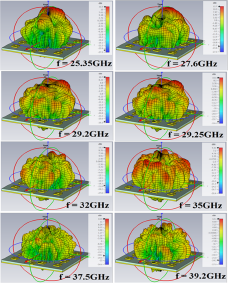
Figure 20. 3D directivity pattern concerning antenna B.

Figure 21. 3D directivity pattern concerning antennae C and D.
E and H planes are crucial in antenna design, influencing polarization. Their role is vital for effective implementation, impacting the overall outcome significantly, and Figs 13–18 represent the E and H planes concerning resonate frequencies as 21.5, 23.8, 27.1, 29, 30.4, 33.66, 37.1, and 39.08 GHz, and 25.35, 27.6, 29.2, 29.25, 32, 35, 37.5, and 39.2 GHz, and 27.32, 33, and 37.86 GHz, and 27.6, 35.36, and 38.86 GHz concerning designs A, B, C, and D, respectively.
Figures 19–21 represent the 3D directivity pattern and peak directivity of 11.3, 13.4, 10.1, and 7.17 dBi concerning resonate frequencies as 21.5, 23.8, 27.1, 29, 30.4, 33.66, 37.1, and 39.08 GHz, and 25.35, 27.6, 29.2, 29.25, 32, 35, 37.5, and 39.2 GHz, and 27.32, 33, and 37.86 GHz, and 27.6, 35.36, and 38.86 GHz concerning designs A, B, C, and D, respectively. Figures 22 and 23 depict the 2D power field pattern concerning Φ = 0°, 90° and θ = 90° with respect to resonate frequencies as 21.5, 23.8, 27.1, 29, 30.4, 33.66, 37.1, and 39.08 GHz, and 25.35, 27.6, 29.2, 29.25, 32, 35, 37.5, and 39.2 GHz, and 27.32, 33, and 37.86 GHz, and 27.6, 35.36, and 38.86 GHz concerning designs A, B, C, and D, respectively.
The 2D pattern signifies the primary lobe direction as the beam direction, crucial for 5G and next-gen communication. In array antenna D, the compact size and sharp notches in the 5G NR band enable effective communication in advanced 5G bands. Figures 22 and 23 depict 2D patterns with distinct notches, addressing sub-6G and advanced 5G network applications, ensuring efficient coverage.

Figure 22. 2D radiation pattern concerning antennae A and B.

Figure 23. 2D radiation pattern concerning antennae C and D.
Fabrication process
The antennae are produced on a Printed Circuit Board (PCB) board utilizing an Fr4 substrate with a relative permittivity (Epsilon) value of 4.3 and permeability (mu) of 1. Standard PCB manufacturing equipment enables the fabrication process, and the substrate has a height of 1.6 mm. In Fig. 24, various perspectives of the structures (array antennae A, B, C, and D) on the Fr4 substrate are depicted, including front, backside, and side diagonal views. The proposed array antennae offer significant size reduction, enhanced directivity, FBR, gain, and bandwidth. Rigorous testing, utilizing a vector network analyzer, power sensor, and spectrum analyzer, confirms the successful design and performance of the proposed antennae.

Figure 24. Fabrication of proposed antenna: front view, back view, and side view of proposed antennae A, B, C, and D with Fr4 substrate.
Experimental results with VNA, power sensor, and spectrum analyzer
Antennae are successfully fabricated and tested in the presence of absorber. Figures 25–27 show the measurement setup and the proposed antenna’s measured result with VNA, power sensor, spectrum analyzer, and radiation in the presence of an absorber. Figures 25–27 represent the measurement with a fabricated prototype antenna through an absorber, VNA, power sensor, and spectrum analyzer. Figures 28–31 depict the measurement results concerning reflection coefficient, phase-group delay, radiation pattern, and fidelity factor [Reference Quintero, Zurcher and Skrivervik23] overall design with different scaling, respectively, and compare results with other existing work against Table 8. Table 6 displays the parameter variations of the proposed antenna, along with the measured results’ return loss and bandwidth percentages. However, Table 7 depicts the specified application coverage for each proposed antenna. The antennae have bandwidths of 0.4, 0.1, 0.24, 0.35, 0.8, and 0.6, 0.6, 0.15, 1.1, 1, and 4, 1.1, 0.900, and 4, 0.05, 0.05, 0.16, 0.100, 1.2, and 1.6 in GHz. The proposed antennae have multiband properties, with resonance frequencies of 19.414, 23.57, 27.67, 28.44, 31.94, 36.4, 19.87, 27.6, 28.8, 31.7, 38.1, 28.09, 31.7, 38.1, 28.09, 31.58, 19.87, 27.16, 28.7, 31.27, 36.97, and 39.28 in GHz and return losses of 20.489, 10.5(Approx.), 10.4 (Approx.), 15.89, 14.37, 15.36,15.9, 12.5, 20.8, 31.2, 25.9, 25.3, 21, 23.4,10.5, 12.8, 15.6, 12.19, 12.9, and 13.16 in dB concerning array antennae A, B, C, and D. The fabricated prototypes are compared with a few other published research works in that the fabricated prototype gets good bandwidth and gain with compact size reduction to cover the expected 6G and 5G band region. The proposed fabricated antennae cover 5G and expected 6G applications with bandwidths of 0.4, 0.1, 0.24, 0.35, 0.8, and 0.6, 0.6, 0.15, 1.1, 1, and 4, 1.1, 0.900, and 4, 0.05, 0.05, 0.16, 0.100, 1.2, and 1.6 in GHz.

Figure 25. Measurement setup for fabricated prototypes of the proposed antennae with VNA.

Figure 26. Measurement of power and measurement setup for fabricated prototype of proposed antennae with power sensor.

Figure 27. Measurement of different parameters and measurement setup for fabricated prototype of proposed antennae with spectrum analyzer.

Figure 28. Measured result of proposed prototypes of antennae A, B, C, and D with VNA.

Figure 29. Measured result of proposed prototypes of antennae A, B, C, and D with VNA.

Figure 30. Measured result of proposed prototypes of antennae in presence of absorber.

Figure 31. Antenna (1) system fidelity factor (2) for proposed prototypes of antennae A, B, C, and D.
Table 6. Comparative study of proposed antenna’s experimental result concerning different parameters

Table 7. Comparative study of proposed antenna’s specific applications concerning resonance frequencies

Table 8. Comparing the outcomes of the proposed antenna with previous research findings across various parameters

Conclusion
The suggested array antennae, inspired by fractals, demonstrate favorable outcomes for covering the sub-6G and advanced 5G band spectrum. Simulated findings indicate a gain increase to 11.04, 11.9, 8.4, and 6 in dBi for proposed designs A, B, C, and D, respectively. The antennae exhibit radiated power with directivities of 11.3, 13.4, 9.29, and 7.17 dBi for the corresponding designs, focusing on slots to enhance radiation. In the mm-wave range, frequency fluctuations are more pronounced, and the current distribution concentrates on fractal slots, boosting antenna radiation. Notably, maximum return losses of 37, 32.8, 31.2, and 23 dB characterize higher radiating capabilities for designs A, B, C, and D.
Moreover, the bandwidths for applications covered in the 5G NR and sub-6G frequency ranges with the bandwidth of 1.92, 0.73, 0.7, 2.4, 1.3, 5.3, and 1.26 GHz, and 3.4, 3.7, 2.67, 4.65 GHz, and 2, 3.5, 1.57 GHz, and 2.5, 1.5, 1.0 GHz concerning designs A, B, C, and D. Angular 3dB width, FBR, and TRP of the proposed antenna depict a noble receiver antenna. The proposed fabricated antennae cover 5G and sub-6G applications with bandwidths of 0.4, 0.1, 0.24, 0.35, and 0.8 GHz, and 0.6, 0.6, 0.15, 1.1, and 1 GHz and 4, 1.1, and 0.900 GHz, and 4, 0.05, 0.05, 0.16, 0.100, 1.2, and 1.6 GHz. The suggested antennae were developed using CST, and their efficacy was successfully validated through testing with the VNA, spectrum analyzer, and power sensor. Exhibiting enhanced radiation within the resonate frequencies ranging from 20 to 40 GHz with Φ = 0°, Φ = 90°, and θ = 90°, these antennae, designed for 5G NR bands, display notable performance. In the mm-wave range, frequency fluctuations are observed, with concentrated current distribution on fractal slots contributing to increased radiation. Notably, the proposed design surpasses existing works in size, gain, and bandwidth and significantly reduces size. Featuring multiband capabilities, the antennae cater to various applications across the n257, n258, n259, n260, and n261 5G NR bands, as well as sub-6G bands, including ground-based radio navigation applications. This innovative design promises versatility and outperforms predecessors in multiple vital aspects.
Data availability statement
Datasets/materials generated during these findings are available on reasonable requests to the corresponding author.
Author contributions
Arun Raj and Durbadal Mandal contributed to this finding. Dr. Mandal supervised this project.
Funding statement
We express gratitude to Science and Engineering Research Board (SERB), Department of Science and Technology, Government of India (Sanction Order No: EEQ/2021/000700; Dated 04 March 2022), for the funding essential for conducting our research.
Competing interests
The authors report no conflict of interest.

Arun Raj, a resident of Uttar Pradesh, graduated in 2020 with a B.Tech in Electronics and Communication Engineering from Chaudhary Charan Singh University (state university), Meerut, Uttar Pradesh, India, and a Master’s from Dr. A P J A Kalam Technical University (state university), Uttar Pradesh, in 2022. He joined for PhD at NIT Durgapur in 2022. He has authored more than seven published and accepted conference papers, and two SCi-indexed journal papers with one self-published book.

Durbadal Mandal (Member, IEEE) received the B.E., M.Tech, and Ph.D. degrees from the National Institute of Technology, Durgapur, West Bengal, India. He is currently attached with the National Institute of Technology, Durgapur, as an Associate Professor with the Department of Electronics and Communication Engineering. He has published more than 400 research papers in international journals and conferences. He has produced 15+ Ph.D. students to date. His research interests include array antenna design and digital filter optimization via evolutionary optimization techniques.


