Skip to main content Accessibility help
×
Hostname: page-component-78c5997874-v9fdk Total loading time: 0 Render date: 2024-11-18T07:38:02.343Z Has data issue: false hasContentIssue false

14 - Nanoscale Deposition and Etching of Materials Using Focused Electron Beams and Liquid Reactants

from Part II - Applications

Published online by Cambridge University Press:  22 December 2016

Frances M. Ross
Affiliation:
IBM T. J. Watson Research Center, New York
Get access

Summary

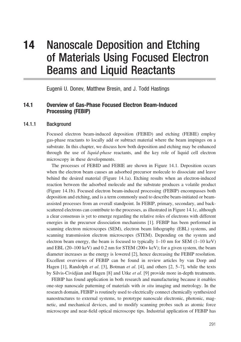
Image of the first page of this content. For PDF version, please use the ‘Save PDF’ preceeding this image.'
Type
Chapter
Information
Publisher: Cambridge University Press
Print publication year: 2016

Access options

Get access to the full version of this content by using one of the access options below. (Log in options will check for institutional or personal access. Content may require purchase if you do not have access.)

References

van Dorp, W. F. and Hagen, C. W., A critical literature review of focused electron beam-induced deposition. J. Appl. Phys., 104 (2008), 081301.Google Scholar
Utke, I., Hoffmann, P. and Melngailis, J., Gas-assisted focused electron beam and ion beam processing and fabrication. J. Vac. Sci. Technol. B, 26 (2008), 11971276.CrossRefGoogle Scholar
Randolph, S. J., Fowlkes, J. D. and Rack, P. D., Focused, nanoscale electron beam-induced deposition and etching. Crit. Rev. Solid State Mater. Sci., 31 (2006), 5589.Google Scholar
Botman, A., Mulders, J. J. L. and Hagen, C. W., Creating pure nanostructures from electron beam-induced deposition using purification techniques: a technology perspective. Nanotechnology, 20 (2009), 372001.CrossRefGoogle ScholarPubMed
Furuya, K., Nanofabrication by advanced electron microscopy using intense and focused beam. Sci. Technol. Adv. Mater., 9 (2008), 014110.CrossRefGoogle ScholarPubMed
Song, M. H. and Furuya, K., Fabrication and characterization of nanostructures on insulator substrates by electron beam-induced deposition. Sci. Technol. Adv. Mater., 9 (2008), 023002.CrossRefGoogle ScholarPubMed
Lee, S. W. and Sankaran, R. M., Direct writing via electron-driven reactions. Mater. Today, 16 (2013), 117122.CrossRefGoogle Scholar
Silvis-Cividjian, N. and Hagen, C. W., Electron Beam-Induced Nanometer-Scale Deposition (San Diego, CA: Academic Press, 2006).CrossRefGoogle Scholar
Utke, I., Moshkalev, S. and Russell, P., Nanofabrication Using Focused Ion and Electron Beams: Principles and Applications (Oxford; New York: Oxford University Press, 2012).Google Scholar
Takahashi, T., Arakawa, Y., Nishioka, M. and Ikoma, T., Selective growth of GaAs wire structures by electron beam-induced metalorganic chemical vapor-deposition. Appl. Phys. Lett., 60 (1992), 6870.CrossRefGoogle Scholar
Crozier, P. A., Tolle, J., Kouvetakis, J. and Ritter, C., Synthesis of uniform GaN quantum dot arrays via electron nanolithography of D2GaN3. Appl. Phys. Lett., 84 (2004), 34413443.CrossRefGoogle Scholar
Che, R. C., Takeguchi, M., Shimojo, M., Zhang, W. and Furuya, K., Fabrication and electron holography characterization of FePt alloy nanorods. Appl. Phys. Lett., 87 (2005), 223109.Google Scholar
Winhold, M., Weirich, P. M., Schwalb, C. H. and Huth, M., Superconductivity and metallic behavior in PbxCyOδ structures prepared by focused electron beam-induced deposition. Appl. Phys. Lett., 105 (2014), 162603.CrossRefGoogle Scholar
Bresin, M., Chamberlain, A., Donev, E. U. et al., Electron beam-induced deposition of bimetallic nanostructures from bulk liquids. Angew. Chem. Int. Ed., 52 (2013), 80048007.CrossRefGoogle ScholarPubMed
Bresin, M., Nadimpally, B. R., Nehru, N., Singh, V. P. and Hastings, J. T., Site-specific growth of CdS nanostructures. Nanotechnology, 24 (2013), 505305.Google Scholar
Bresin, M., Nehru, N. and Hastings, J. T., Focused electron beam-induced deposition of plasmonic nanostructures from aqueous solutions. In Proc. SPIE 8613, Advanced Fabrication Technologies for Micro/Nano Optics and Photonics VI (2013), p. 861306.Google Scholar
Chen, X., Zhou, L. H., Wang, P. et al., A study of electron beam-induced deposition and nano device fabrication using liquid cell TEM technology. Chinese J. Chem., 32 (2014), 399404.Google Scholar
Chen, X., Zhou, L. H., Wang, P., Zhao, C. J. and Miao, X. L., A study of nano materials and their reactions in liquid using in situ wet cell TEM technology. Chinese J. Chem., 30 (2012), 28392843.Google Scholar
den Heijer, M., Shao, I., Radisic, A., Reuter, M. C. and Ross, F. M., Patterned electrochemical deposition of Cu using an electron beam. APL Mater., 2 (2014), 022101.Google Scholar
Donev, E. U. and Hastings, J. T., Liquid-precursor electron beam-induced deposition of Pt nanostructures: dose, proximity, resolution. Nanotechnology, 20 (2009), 505302.Google Scholar
Donev, E. U. and Hastings, J. T., Electron beam-induced deposition of Pt from a liquid precursor. Nano Lett., 9 (2009), 27152718.Google Scholar
Donev, E. U., Schardein, G., Wright, J. C. and Hastings, J. T., Substrate effects on the electron beam-induced deposition of Pt from a liquid precursor. Nanoscale, 3 (2011), 27092717.CrossRefGoogle ScholarPubMed
Grogan, J. M., Schneider, N. M., Ross, F. M. and Bau, H. H., Bubble and pattern formation in liquid induced by an electron beam. Nano Lett., 14 (2014), 359364.Google Scholar
Hoshino, T. and Morishima, K., Electron beam direct processing on living cell membrane. Appl. Phys. Lett., 99 (2011), 174102.CrossRefGoogle Scholar
Jensen, E., Kobler, C., Jensen, P. S. and Molhave, K., In-situ SEM microchip setup for electrochemical experiments with water based solutions. Ultramicroscopy, 129 (2013), 6369.CrossRefGoogle ScholarPubMed
Kolmakova, N. and Kolmakov, A., Scanning electron microscopy for in situ monitoring of semiconductor-liquid interfacial processes: electron assisted reduction of Ag ions from aqueous solution on the surface of TiO2 rutile nanowire. J. Phys. Chem. C, 114 (2010), 1723317237.Google Scholar
Kraus, T. and de Jonge, N., Dendritic Au nanowire growth observed in liquid with transmission electron microscopy. Langmuir, 29 (2013), 84278432.Google Scholar
Liu, Y., Chen, X., Noh, K. W. and Dillon, S. J., Electron beam-induced deposition of silicon nanostructures from a liquid phase precursor. Nanotechnology, 23 (2012), 385302.Google Scholar
Liu, Y., Tai, K. P. and Dillon, S. J., Growth kinetics and morphological evolution of ZnO precipitated from solution. Chem. Mater., 25 (2013), 29272933.Google Scholar
Noh, K. W., Liu, Y., Sun, L. and Dillon, S. J., Challenges associated with in-situ TEM in environmental systems: the case of silver in aqueous solutions. Ultramicroscopy, 116 (2012), 3438.Google Scholar
Ocola, L. E., Joshi-Imre, A., Kessel, C. et al., Growth characterization of electron beam-induced silver deposition from liquid precursor. J. Vac. Sci. Technol. B, 30 (2012), 06FF08.CrossRefGoogle Scholar
Schardein, G., Donev, E. U. and Hastings, J. T., Electron beam-induced deposition of Au from aqueous solutions. Nanotechnology, 22 (2011), 015301.Google Scholar
Woehl, T. J., Evans, J. E., Arslan, L., Ristenpart, W. D. and Browning, N. D., Direct in situ determination of the mechanisms controlling nanoparticle nucleation and growth. ACS Nano, 6 (2012), 85998610.CrossRefGoogle ScholarPubMed
Yuk, J. M., Park, J., Ercius, P. et al., High-resolution EM of colloidal nanocrystal growth using graphene liquid cells. Science, 336 (2012), 6164.CrossRefGoogle ScholarPubMed
Zheng, H. M., Smith, R. K., Jun, Y. W. et al., Observation of single colloidal Pt nanocrystal growth trajectories. Science, 324 (2009), 13091312.CrossRefGoogle Scholar
Donev, E. U., Nehru, N., Schardein, G. et al., Recent advances in liquid-phase electron beam-induced deposition: characterizing growth processes and optical properties. Microsc. Microanal., 17 (2011), 438439.CrossRefGoogle Scholar
Randolph, S. J., Botman, A. and Toth, M., Capsule-free fluid delivery and beam-induced electrodeposition in a scanning electron microscope. RSC Adv., 3 (2013), 2001620023.Google Scholar
Bresin, M., Botman, A., Randolph, S. J., Straw, M. and Hastings, J. T., Liquid phase electron beam-induced deposition on bulk substrates using environmental scanning electron microscopy. Microsc. Microanal., 20 (2014), 376384.Google Scholar
Tsuda, T., Seino, S. and Kuwabata, S., Au nanoparticles prepared with a room-temperature ionic liquid-radiation irradiation method. Chem. Commun., 44 (2009), 67926794.Google Scholar
Roy, P., Lynch, R. and Schmuki, P., Electron beam-induced in-vacuo Ag deposition on TiO2 from ionic liquids. Electrochem. Commun., 11 (2009), 15671570.Google Scholar
Imanishi, A., Tamura, M. and Kuwabata, S., Formation of Au nanoparticles in an ionic liquid by electron beam irradiation. Chem. Commun., 44 (2009), 17751777.Google Scholar
Imanishi, A., Gonsui, S., Tsuda, T., Kuwabata, S. and Fukui, K., Size and shape of Au nanoparticles formed in ionic liquids by electron beam irradiation. Phys. Chem. Chem. Phys., 13 (2011), 1482314830.Google Scholar
de Jonge, N., Introduction to special issue on electron microscopy of specimens in liquid. Microsc. Microanal., 20 (2014), 315316.CrossRefGoogle ScholarPubMed
de Jonge, N., and Ross, F. M., Electron microscopy of specimens in liquid. Nat. Nanotechnol., 6 (2011), 695704.Google Scholar
Thiberge, S., Zik, O. and Moses, E., An apparatus for imaging liquids, cells, and other wet samples in the scanning electron microscope. Rev. Sci. Instrum., 75 (2004), 22802289.Google Scholar
Ciarlo, D. R., Silicon nitride thin windows for biomedical microdevices. Biomed. Microdevices, 4 (2002), 6368.CrossRefGoogle Scholar
Stelmashenko, N. A., Craven, J. P., Donald, A. M., Terentjev, E. M. and Thiel, B. L., Topographic contrast of partially wetting water droplets in environmental scanning electron microscopy. J. Microsc. Oxford, 204 (2001), 172183.Google Scholar
Botman, A., Mulders, J. J. L., Weemaes, R. and Mentink, S., Purification of Pt and Au structures after electron beam-induced deposition. Nanotechnology, 17 (2006), 37793785.CrossRefGoogle Scholar
Langford, R. M., Wang, T. X. and Ozkaya, D., Reducing the resistivity of electron and ion beam assisted deposited Pt. Microelectron. Eng., 84 (2007), 784788.Google Scholar
Lin, J. F., Bird, J. P., Rotkina, L. and Bennett, P. A., Classical and quantum transport in focused-ion beam-deposited Pt nanointerconnects. Appl. Phys. Lett., 82 (2003), 802804.CrossRefGoogle Scholar
Penate-Quesada, L., Mitra, J. and Dawson, P., Non-linear electronic transport in Pt nanowires deposited by focused ion beam. Nanotechnology, 18 (2007), 215203.Google Scholar
Tao, T., Ro, J. S., Melngailis, J., Xue, Z. L. and Kaesz, H. D., Focused ion beam-induced deposition of Pt. J. Vac. Sci. Technol. B, 8 (1990), 18261829.Google Scholar
Telari, K. A., Rogers, B. R., Fang, H. et al., Characterization of Pt films deposited by focused ion beam-assisted chemical vapor deposition. J. Vac. Sci. Technol. B, 20 (2002), 590595.Google Scholar
Ritchie, N. W. M., Spectrum simulation in DTSA-II. Microsc. Microanal., 15 (2009), 454468.Google Scholar
Ritchie, N. W. M., Using DTSA-II to simulate and interpret energy dispersive spectra from particles. Microsc. Microanal., 16 (2010), 248258.Google Scholar
Folch, A., Servat, J., Esteve, J., Tejada, J. and Seco, M., High-vacuum versus “environmental” electron beam deposition. J. Vac. Sci. Technol. B, 14 (1996), 26092614.CrossRefGoogle Scholar
Brintlinger, T., Fuhrer, M. S., Melngailis, J. et al., Electrodes for carbon nanotube devices by focused electron beam-induced deposition of Au. J. Vac. Sci. Technol. B, 23 (2005), 31743177.CrossRefGoogle Scholar
Green, T. A., Au electrodeposition for microelectronic, optoelectronic and microsystem applications. Gold Bull., 40 (2007), 105114.CrossRefGoogle Scholar
Friedli, V., Utke, I., Molhave, K. and Michler, J., Dose and energy dependence of mechanical properties of focused electron beam-induced pillar deposits from Cu(C5HF6O2)2. Nanotechnology, 20 (2009), 385304.Google Scholar
Ochiai, Y., Fujita, J. and Matsui, S., Electron beam-induced deposition of Cu compound with low resistivity. J. Vac. Sci. Technol. B, 14 (1996), 38873891.CrossRefGoogle Scholar
Kunz, R. R. and Mayer, T. M., Electron beam-induced surface nucleation and low-temperature decomposition of metal-carbonyls. J. Vac. Sci. Technol. B, 6 (1988), 15571564.Google Scholar
Chamberlain, A., Donev, E. U., Samantaray, C. B. et al., Electron beam-induced deposition of transition metals from bulk liquids: Ag, Cr, and Ni. In 55th International Conference on Electron, Ion, and Photon Beam Technology and Nanofabrication (Las Vegas, NV, 2011).Google Scholar
Spoddig, D., Schindler, K., Rodiger, P. et al., Transport properties and growth parameters of PdC and WC nanowires prepared in a dual-beam microscope. Nanotechnology, 18 (2007), 495202.Google Scholar
Anbar, M. and Neta, P., A compilation of specific bimolecular rate constants for the reactions of hydrated electrons, hydrogen atoms and hydroxyl radicals with inorganic and organic compounds in aqueous solution. Int. J. Appl. Radiat. Isot., 18 (1967), 493523.CrossRefGoogle Scholar
Hayes, D., Micic, O. I., Nenadovic, M. T., Swayambunathan, V. and Meisel, D., Radiolytic production and properties of ultrasmall cadmium sulfide particles. J. Phys. Chem., 93 (1989), 46034608.Google Scholar
Wu, M. H., Zhong, H. J., Jiao, Z., Li, Z. and Sun, Y. F., Synthesis of PbS nanocrystallites by electron beam irradiation. Coll. Surf. A, 313 (2008), 3539.CrossRefGoogle Scholar
Evans, J. E., Jungjohann, K. L., Browning, N. D. and Arslan, I., Controlled growth of nanoparticles from solution with in situ liquid transmission electron microscopy. Nano Lett., 11 (2011), 28092813.Google Scholar
Roediger, P., Hochleitner, G., Bertagnolli, E., Wanzenboeck, H. D. and Buehler, W., Focused electron beam-induced etching of silicon using chlorine. Nanotechnology, 21 (2010), 285306.CrossRefGoogle ScholarPubMed
Roediger, P., Wanzenboeck, H. D., Hochleitner, G., Bertagnolli, E. and Buehler, W., Focused electron beam-induced etching of silicon by chlorine gas: negative effects of residual gas contamination on the etching process. J. Appl. Phys., 108 (2010), 124316.Google Scholar
Martin, A. A. and Toth, M., Cryogenic electron beam-induced chemical etching. ACS Appl. Mater. Inter., 6 (2014), 1845718460.Google Scholar
Roediger, P., Mijic, M., Zeiner, C. et al., Local, direct-write, damage-free thinning of germanium nanowires. J. Vac. Sci. Technol. B, 29 (2011), 06FB03.Google Scholar
Roediger, P., Wanzenboeck, H. D., Hochleitner, G. and Bertagnolli, E., Crystallinity-retaining removal of germanium by direct-write focused electron beam-induced etching. J. Vac. Sci. Technol. B, 29 (2011), 041801.Google Scholar
Fox, D., O’Neill, A., Zhou, D. et al., Nitrogen assisted etching of graphene layers in a scanning electron microscope. Appl. Phys. Lett., 98 (2011), 243117.Google Scholar
Bret, T., Afra, B., Becker, R. et al., Gas assisted focused electron beam-induced etching of alumina. J. Vac. Sci. Technol. B, 27 (2009), 27272731.CrossRefGoogle Scholar
Spinney, P. S., Howitt, D. G., Smith, R. L. and Collins, S. D., Nanopore formation by low-energy focused electron beam machining. Nanotechnology, 21 (2010), 375301.Google Scholar
Ganczarczyk, A., Geller, M. and Lorke, A., XeF2 gas-assisted focused-electron beam-induced etching of GaAs with 30 nm resolution. Nanotechnology, 22 (2011), 045301.Google Scholar
Noh, J. H., Fowlkes, J. D., Timilsina, R. et al., Pulsed laser-assisted focused electron beam-induced etching of titanium with XeF2: enhanced reaction rate and precursor transport. ACS Appl. Mater. Inter., 7 (2015), 41794184.Google Scholar
Schoenaker, F. J., Cordoba, R., Fernandez-Pacheco, R. et al., Focused electron beam-induced etching of titanium with XeF2. Nanotechnology, 22 (2011), 265304.Google Scholar
Toth, M., Advances in gas-mediated electron beam-induced etching and related material processing techniques. Appl. Phys. A, 117 (2014), 16231629.Google Scholar
Coburn, J. W. and Winters, H. F., Ion-assisted and electron-assisted gas-surface chemistry: important effect in plasma-etching. J. Appl. Phys., 50 (1979), 31893196.Google Scholar
Yemini, M., Hadad, B., Liebes, Y., Auner, A. and Ashkenasy, N., The controlled fabrication of nanopores by focused electron beam-induced etching. Nanotechnology, 20 (2009), 245302.Google Scholar
Liebes, Y., Hadad, B. and Ashkenasy, N., Effects of electrons on the shape of nanopores prepared by focused electron beam-induced etching. Nanotechnology, 22 (2011), 285303.Google Scholar
Crozier, P. A., Nanoscale oxide patterning with electron-solid-gas reactions. Nano Lett., 7 (2007), 23952398.Google Scholar
Dekker, C., Solid-state nanopores. Nat. Nanotechnol., 2 (2007), 209215.Google Scholar
Donev, E. U., Samantaray, C. B., Bresin, M. and Hastings, J. T., Recent advances in liquid-phase e-beam-induced processing: silicon nitride etching and palladium deposition. In 39th International Conference on Micro and Nano Engineering (London, 2013), p. O-FEBIP-04.Google Scholar
Drezner, Y., Greenzweig, Y. and Raveh, A., Strategy for focused ion beam compound material removal for circuit editing. J. Vac. Sci. Technol. B, 30 (2012), 011207.Google Scholar
Jaeckervoirol, A., Ponche, J. L. and Mirabel, P., Vapor-pressures in the ternary-system water nitric-acid sulfuric-acid at low-temperatures. J. Geophys. Res. Atmos., 95 (1990), 1185711863.Google Scholar
Bresin, M. and Hastings, J. T., Etching of Cu using liquid reactants and a focused electron beam. In International Conference on Electron, Ion, and Photon Beam Technology and Nanofabrication (Washington, D.C., 2014).Google Scholar
Massucci, M., Clegg, S. L. and Brimblecombe, P., Equilibrium vapor pressure of H2O above aqueous H2SO4 at low temperature. J. Chem. Eng. Data, 41 (1996), 765778.CrossRefGoogle Scholar

Save book to Kindle

To save this book to your Kindle, first ensure coreplatform@cambridge.org is added to your Approved Personal Document E-mail List under your Personal Document Settings on the Manage Your Content and Devices page of your Amazon account. Then enter the ‘name’ part of your Kindle email address below. Find out more about saving to your Kindle.

Note you can select to save to either the @free.kindle.com or @kindle.com variations. ‘@free.kindle.com’ emails are free but can only be saved to your device when it is connected to wi-fi. ‘@kindle.com’ emails can be delivered even when you are not connected to wi-fi, but note that service fees apply.

Find out more about the Kindle Personal Document Service.

Available formats
×

Save book to Dropbox

To save content items to your account, please confirm that you agree to abide by our usage policies. If this is the first time you use this feature, you will be asked to authorise Cambridge Core to connect with your account. Find out more about saving content to Dropbox.

Available formats
×

Save book to Google Drive

To save content items to your account, please confirm that you agree to abide by our usage policies. If this is the first time you use this feature, you will be asked to authorise Cambridge Core to connect with your account. Find out more about saving content to Google Drive.

Available formats
×