Hostname: page-component-586b7cd67f-t8hqh Total loading time: 0 Render date: 2024-12-01T06:15:43.011Z Has data issue: false hasContentIssue false

Investigating surface effects of GaN nanowires using confocal microscopy at below-band gap excitation

Published online by Cambridge University Press:  09 October 2017

Lauren R. Richey-Simonsen
Affiliation:
Department of Physics & Astronomy, University of Utah, Salt Lake City, Utah 84112, USA
Nicholas J. Borys
Affiliation:
Department of Physics & Astronomy, University of Utah, Salt Lake City, Utah 84112, USA; and Molecular Foundry, Lawrence Berkeley National Laboratory, Berkeley, California 94720, USA
Tevye R. Kuykendall
Affiliation:
Molecular Foundry, Lawrence Berkeley National Laboratory, Berkeley, California 94720, USA
P. James Schuck
Affiliation:
Molecular Foundry, Lawrence Berkeley National Laboratory, Berkeley, California 94720, USA
Shaul Aloni
Affiliation:
Molecular Foundry, Lawrence Berkeley National Laboratory, Berkeley, California 94720, USA
Jordan M. Gerton*
Affiliation:
Department of Physics & Astronomy, University of Utah, Salt Lake City, Utah 84112, USA
*
a) Address all correspondence to this author. e-mail: jgerton@physics.utah.edu
Get access

Abstract

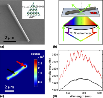
We analyze the microscopic origins of subgap photoexcitations of individual gallium nitride (GaN) triangular cross-section nanowires (NWs), which are highly photoactive over a broadband spectral range. Using confocal hyperspectral photoluminescence (PL) microscopy, mid-gap states on the NWs were excited using subgap illumination, resulting in two distinct PL spectra corresponding to the polar (0001) and the semipolar $\left( {\bar 1101} \right)$ / $\left( {1\bar 101} \right)$ surfaces. Emission spectra are well represented by Gaussian functions with fitted centers of 1.99 ± 0.01 eV and 2.26 ± 0.01 eV, respectively. PL collected from the end facets exhibits interference fringes and a relative blue shift. Furthermore, the PL spectrum shifts strongly to the blue when the excitation intensity is increased. These observations are consistent with a qualitative model in which the PL results from excitation into a broad manifold of surface-associated states which are rapidly populated at a high excitation intensity and can couple to etalon modes via longitudinal photon emission.

Type
Invited Articles
Copyright
Copyright © Materials Research Society 2017 

Access options

Get access to the full version of this content by using one of the access options below. (Log in options will check for institutional or personal access. Content may require purchase if you do not have access.)

Footnotes

Contributing Editor: Johan Brand Malherbe

References

REFERENCES

Reshchikov, M.A. and Morkoc, H.: Luminescence properties of defects of GaN. J. Appl. Phys. 97, 061310 (2005).Google Scholar
Philipps, J.M., Müntze, G.M., Hille, P., Wallys, J., Schörmann, J., Teubert, J., Hofmann, D.M., and Eickhoff, M.: Radical formation at the gallium nitride nanowire–electrolyte interface by photoactivated charge transfer. Nanotechnology 24(32), 325701 (2013).Google Scholar
Slimane, A.B., Najar, A., Elafandy, R., San-Román-Alerigi Dá, P., Anjum, D., Ng, T.K., and Ooi, B.S.: On the phenomenon of large photoluminescence red shift in GaN nanoparticles. Nanoscale Res. Lett. 8(1), 342 (2013).Google Scholar
Goldberger, J., He, R., Zhang, Y., Lee, S., Yan, H., Choi, H-J., and Yang, P.: Single-crystal gallium nitride nanotubes. Nature 422(6932), 599 (2003).Google Scholar
Kuykendall, T., Pauzauskie, P.J., Zhang, Y., Goldberger, J., Sirbuly, D., Denlinger, J., and Yang, P.: Crystallographic alignment of high-density gallium nitride nanowire arrays. Nat. Mater. 3(8), 524 (2004).Google Scholar
Zhang, J., Zhang, L.D., Wang, X.F., Liang, C.H., Peng, X.S., and Wang, Y.W.: Fabrication and photoluminescence of ordered GaN nanowire arrays. J. Chem. Phys. 115(13), 5714 (2001).CrossRefGoogle Scholar
Nguyen, H.P.T., Zhang, S., Cui, K., Han, X., Fathololoumi, S., Couillard, M., Botton, G.A., and Mi, Z.: p-Type modulation doped InGaN/GaN dot-in-a-wire white-light-emitting diodes monolithically grown on Si(111). Nano Lett. 11(5), 1919 (2011).Google Scholar
Schwartzberg, A.M., Aloni, S., Kuykendall, T., Schuck, P.J., and Urban, J.J.: Optical cavity characterization in nanowires via self-generated broad-band emission. Opt. Express 19(9), 8903 (2011).Google Scholar
Sanders, A., Blanchard, P., Bertness, K., Brubaker, M., Dodson, C., Harvey, T., Herrero, A., Rourke, D., Schlager, J., Sanford, N., Chiaramonti, A.N., Davydov, A., Motayed, A., and Tsvetkov, D.: Homoepitaxial n-core:p-shell gallium nitride nanowires: HVPE overgrowth on MBE nanowires. Nanotechnology 22(46), 465703 (2011).Google Scholar
Kuykendall, T., Aloni, S., Jen-La Plante, I., and Mokari, T.: Growth of GaN@InGaN core–shell and Au–GaN hybrid nanostructures for energy applications. Int. J. Photoenergy 2009, 1 (2009).CrossRefGoogle Scholar
Lähnemann, J., Hauswald, C., Wölz, M., Jahn, U., Hanke, M., Geelhaar, L., and Brandt, O.: Localization and defects in axial (In,Ga)N/GaN nanowire heterostructures investigated by spatially resolved luminescence spectroscopy. J. Phys. D: Appl. Phys. 47(39), 394010 (2014).CrossRefGoogle Scholar
Zhao, S., Kibria, M.G., Wang, Q., Nguyen, H.P.T., and Mi, Z.: Growth of large-scale vertically aligned GaN nanowires and their heterostructures with high uniformity on SiO x by catalyst-free molecular beam epitaxy. Nanoscale 5(12), 5283 (2013).CrossRefGoogle ScholarPubMed
Ohno, T., Bai, L., Hisatomi, T., Maeda, K., and Domen, K.: Photocatalytic water splitting using modified GaN:ZnO solid solution under visible light: Long-time operation and regeneration of activity. J. Am. Chem. Soc. 134(19), 8254 (2012).Google Scholar
Sheetz, R.M., Richter, E., Andriotis, A.N., Lisenkov, S., Pendyala, C., Sunkara, M.K., and Menon, M.: Visible-light absorption and large band-gap bowing of GaN1−x Sb x from first principles. Phys. Rev. B 84(7), 075304 (2011).Google Scholar
Akimov, A.V., Muckerman, J.T., and Prezhdo, O.V.: Nonadiabatic dynamics of positive charge during photocatalystic water splitting on GaN(10–10) surface: Charge localization governs splitting efficiency. J. Am. Chem. Soc. 135(23), 8682 (2013).CrossRefGoogle Scholar
Neaton, J. and Zayak, A.T.: Berkeley Lab, Molecular Foundry, Berkeley, CA. Personal Communication, 2015.Google Scholar
Abe, R.: Recent progress on photocatalytic and photoelectrochemical water splitting under visible light irradiation. J. Photochem. Photobiol., C 11(4), 179 (2010).Google Scholar
Qiu, J., Zeng, G., Ha, M-A., Ge, M., Lin, Y., Hettick, M., Hou, B., Alexandrova, A.N., Javey, A., and Cronin, S.B.: Artificial photosynthesis on TiO2-passivated InP nanopillars. Nano Lett. 15(9), 6177 (2015).Google Scholar
Singh, R., Molnar, R.J., Ünlü, M.S., and Moustakas, T.D.: Intensity dependence of photoluminescence in GaN thin films. Appl. Phys. Lett. 64(3), 336 (1994).CrossRefGoogle Scholar
Ponce, F.A., Bour, D.P., Götz, W., and Wright, P.J.: Spatial distribution of the luminescence in GaN thin films. Appl. Phys. Lett. 68(1), 57 (1996).Google Scholar
Li, Q. and Wang, G.T.: Spatial distribution of defect luminescence in GaN nanowires. Nano Lett. 10(5), 1554 (2010).Google Scholar
Upadhya, P.C., Li, Q., Wang, G.T., Fischer, A.J., Taylor, A.J., and Prasankumar, R.P.: The influence of defect states on non-equilibrium carrier dynamics in GaN nanowires. Semicond. Sci. Technol. 25(2), 024017 (2010).Google Scholar
Wang, G.T., Talin, A.A., Werder, D.J., Creighton, J.R., Lai, E., Anderson, R.J., and Arslan, I.: Highly aligned, template-free growth and characterization of vertical GaN nanowires on sapphire by metal–organic chemical vapour deposition. Nanotechnology 17(23), 5773 (2006).Google Scholar
Reshchikov, M.A., Morkoç, H., Park, S.S., and Lee, K.Y.: Yellow and green luminescence in a freestanding GaN template. Appl. Phys. Lett. 78(20), 3041 (2001).Google Scholar
Toda, Y., Matsubara, T., Morita, R., Yamashita, M., Hoshino, K., Someya, T., and Arakawa, Y.: Two-photon absorption and multiphoton-induced photoluminescence of bulk GaN excited below the middle of the band gap. Appl. Phys. Lett. 82(26), 4714 (2003).Google Scholar
Schuck, P.J., Grober, R.D., Roskowski, A.M., Einfeldt, S., and Davis, R.F.: Cross-sectional imaging of pendeo-epitaxial GaN using continuous-wave two-photon microphotoluminescence. Appl. Phys. Lett. 81(11), 1984 (2002).Google Scholar
Chin, A.H., Ahn, T.S., Li, H., Vaddiraji, S., Bardeen, C.J., Ning, C., and Sunkara, M.K.: Photoluminescence of GaN nanowires of different crystallographic orientations. Nano Lett. 7(3), 626 (2007).Google Scholar
Xu, S., Hao, Y., Zhang, J., Jiang, T., Yang, L., Lu, X., and Lin, Z.: Yellow luminescence of polar and nonpolar GaN nanowires on r-plane sapphire by metal organic chemical vapor deposition. Nano Lett. 13(8), 3654 (2013).Google Scholar
Chen, C-C., Yeh, C-C., Chen, C-H., Yu, M-Y., Liu, H-L., Wu, J-J., Chen, K-H., Chen, L-C., Peng, J-Y., and Chen, Y-F.: Catalytic growth and characterization of gallium nitride nanowires. J. Am. Chem. Soc. 123(12), 2791 (2001).Google Scholar
Bao, W., Melli, M., Caselli, N., Riboli, F., Wiersma, D.S., Staffaroni, M., Choo, H., Ogletree, D.F., Aloni, S., Bokor, J., Cabrini, S., Intonti, F., Salmeron, M.B., Yablonovitch, E., Schuck, P.J., and Weber-Bargioni, A.: Mapping local charge recombination heterogeneity by multidimensional nanospectroscopic imaging. Science 338, 1317 (2012).Google Scholar
Kuykendall, T.R., Altoe, M.V.P., Ogletree, D.F., and Aloni, S.: Catalyst-directed crystallographic orientation control of GaN nanowire growth. Nano Lett. 14, 6767 (2014).Google Scholar
Van de Walle, C.G. and Segev, D.: Microscopic origins of surface states on nitride surfaces. J. Appl. Phys. 101(8), 081704 (2007).Google Scholar
Lakowicz, J.R.: Principles of Fluorescence Spectroscopy, 2nd ed. (Kluwer Academic/Plenum Publishers, New York, NY, 1999); p. 58.Google Scholar
Novotny, L. and Hecht, B.: Principles of Nano-Optics (Cambridge University Press, Cambridge, England, 2006); pp. 33351.Google Scholar
Catchpole, K.R. and Polman, A.: Plasmonic solar cells. Opt. Express 16(26), 21793 (2008).Google Scholar
Pennanen, A.M. and Toppari, J.J.: Direct optical measurement of light coupling into planar waveguide by plasmonic nanoparticles. Opt. Express 21(S1), A23 (2013).Google Scholar
Reshchikov, M.A., Demchenko, D.O., Usikov, A., Helava, H., and Makarov, Y.: Identification of point defects in HVPE-grown GaN by steady-state and time-resolved photoluminescence. In Gallium Nitride Materials and Devices X, Chyi, J.-I., Fujioka, H., and Morkoc, H., eds. (Proceedings of SPIE 9363, Bellingham, Washington, 2015), p. 93630L.Google Scholar
Reshchikov, M.A., Morkoç, H., Park, S.S., and Lee, K.Y.: Two charge states of dominant acceptor in unintentionally doped GaN: Evidence from photoluminescence study. Appl. Phys. Lett. 81(26), 4970 (2002).Google Scholar
Lyons, J.L., Alkauskas, A., Janotti, A., and Van de Walle, C.G.: First-principles theory of acceptors in nitride semiconductors. Phys. Status Solidi B 252(5), 900 (2015).Google Scholar
Demchenko, D.O., Diallo, I.C., and Reshchikov, M.A.: Yellow luminescence of gallium nitride generated by carbon defect complexes. Phys. Rev. Lett. 110(8), 087404 (2013).Google Scholar
Lyons, J.L., Janotti, A., and Van de Walle, C.G.: Carbon impurities and the yellow luminescence in GaN. Appl. Phys. Lett. 97(15), 152108 (2010).Google Scholar
Kucheyev, S.O., Toth, M., Phillips, M.R., Williams, J.S., Jagadish, C., and Li, G.: Chemical origin of the yellow luminescence in GaN. J. Appl. Phys. 91(9), 5867 (2002).Google Scholar
Dhara, S., Datta, A., Wu, C.T., Lan, Z.H., Chen, K.H., Wang, Y.L., Chen, Y.F., Hsu, C.W., Chen, L.C., Lin, H.M., and Chen, C.C.: Blueshift of yellow luminescence band in self-ion-implanted n-GaN nanowire. Appl. Phys. Lett. 84(18), 3486 (2004).Google Scholar
Reshchikov, M.A., Visconti, P., and Morkoc, H.: Blue photoluminescence activated by surface states in GaN grown by molecular beam epitaxy. Appl. Phys. Lett. 78, 177 (2001).CrossRefGoogle Scholar
Zhang, X., Zhang, X., Xu, J., Shan, X., Xu, J., and Yu, D.: Whispering gallery modes in single triangular ZnO nanorods. Opt. Lett. 34(16), 2533 (2009).Google Scholar
Kibria, M.G., Zhao, S., Chowdhury, F.A., Wang, Q., Nguyen, H.P.T., Trudeau, M.L., Guo, H., and Mi, Z.: Tuning the surface Fermi level on p-type gallium nitride nanowires for efficient overall water splitting. Nat. Commun. 5, 3825 (2014).Google Scholar
Tian, W., Zhao, C., Leng, J., Cui, R., and Jin, S.: Visualizing carrier diffusion in individual single-crystal organolead halide perovskite nanowires and nanoplates. J. Am. Chem. Soc. 137(39), 12458 (2015).Google Scholar
Shafran, E., Mangum, B.D., and Gerton, J.M.: Using the near-field coupling of a sharp tip to tune fluorescence-emission fluctuations during quantum-dot blinking. Phys. Rev. Lett. 107(3), 037403 (2011).Google Scholar
Supplementary material: PDF

Richey-Simonsen et al supplementary material

Richey-Simonsen et al supplementary material 1

Download Richey-Simonsen et al supplementary material(PDF)
PDF 2.3 MB