0 0) GaN. This orientation would have a misfit of only −1.4% along the
 1. Introduction
The lack of a lattice-matched substrate for epitaxial growth of GaN films has stimulated an intense search for suitable materials. The most commonly used substrate, sapphire, has a very large misfit for GaN, −13.7%. Several alternatives to sapphire have been explored, including SiC Reference Lin, Sverdlov, Zhou and Morkoc[1], spinel Reference Manasevit, Erdmann and Simpson[2], ZnO Reference Hamdani, Botchkarev, Kim, Morkoc, Yeadon, Gibson, Tsen, Smith, Reynolds, Look, Evans, Litton, Mitchel and Hemenger[3] Reference Hellman, Buchanan, Wiesmann and Brener[4], β-LiGaO2 Reference Kung, Saxler, Zhang, Walker, Lavado and Razeghi[5] Reference Trager-Cowan, Middleton and O’Donnell[6], and γ-LiAlO2 Reference Chai[7]. β-LiGaO2 was an obviously promising possibility for GaN epitaxy, because its crystal structure is just a wurtzite superstructure and could be grown by the Czochralski technique. Reference Remeika and Ballman[8] However, β-LiGaO2 may not be sufficiently stable, particularly at the high temperatures used for MOCVD growth, to be advantageous for GaN growth, and the results that have been obtained with it have been mixed. Reference Johnson, Fujita and Rowland[9]
γ-LiAlO2 Footnote [a] is chemically similar to β-LiGaO2. Although the structure Reference Marezio[10] is not as closely related to wurtzite, its higher melting point (1700°C Reference Strickler and Roy[11] vs. 1595°C for β-LiGaO2 Reference Weise and Neumann[12]) and the possibility of Czochralski growth Reference Chai[7] have led some crystal growers to pursue its commercial development. Figure 1 shows the crystal structure of tetragonal γ-LiAlO2. The structure is chiral. The structure can be thought of as a layering of wurzite {1

Figure 1a. Crystal structure of γ-LiAlO2, viewed along the <0 0 1> azimuth.

Figure 1b. (0 1
In this paper we examine the orientation relationships and microstructure for GaN and AlN films grown directly on γ-LiAlO2. We find that the expected orientation relationship does not occur; instead, c-oriented GaN grows with a small tilt towards the γ-LiAlO2 c-axis. We suggest that this tilt is driven by interface energies rather than strain.
2. Epitaxial Growth
The films described here were grown by plasma-assisted molecular beam epitaxy on quarters of a 2 inch (1 0 0) γ-LiAlO2 substrate provided by Crystal Photonics, Inc. Footnote [b] The substrates were cleaned in acetone and methanol, then soldered onto molybdenum heater blocks with indium. The substrates were outgassed at 750°C in vacuum before growth. A normal amount of oxygen outgassing was observed during this stage, and no Li was observed by quadrupole mass spectroscopy. Moderately sharp (1 × 1) reflection high energy electron diffraction (RHEED) patterns, such as shown in Figure 2, were observed from the substrates. It was noted that exposure to the 7.5 keV electron beam resulted in a darkening of a γ-LiAlO2 substrate. This radiation induced coloring is common in materials with very light elements such as lithium.

Figure 2. Reflection high energy electron diffraction (RHEED) patterns observed on the γ-LiAlO2 substrate before growth. (a) <0 0 1> azimuth (b) <0 1 0> azimuth
GaN was grown using Ga rich conditions similar to those we have previously reported. Reference Hellman, Brandle, Schneemeyer, Wiesmann, Brener, Siegrist, Berkstresser, Buchanan and Hartford[13] An RF-coupled nitrogen plasma was used to obtain active nitrogen for MBE growth. A minimal nitridation period of about 10 seconds was used before starting GaN growth. During the time when these films were grown, cross-contamination of our Ga and Mg effusion cells resulted in moderately high Mg doping levels. Silicon contamination from the quartz tube of the plasma source was also present. The substrate temperature for GaN growth was 600°C, and the typical growth rates and film thicknesses were 0.2μm/hr and 0.5 μm, respectively.
We also grew AlN films and GaN films with AlN buffer layers on γ-LiAlO2. The quality of these films was not as good as the GaN films grown directly on LiAlO2., as judged by sharpness of RHEED patterns. When grown as a buffer layer, the AlN was grown at a rate of about 0.02μm/hr at a nominal substrate temperature of 550°C; when grown as a thick layer, the growth rate was 0.24 μm/hr at 650°C.
GaN growth was initiated using a Ga flux set to obtain a growth rate of 0.13 μm/hr on sapphire substrates. The substrate RHEED pattern persisted during the initial stages of growth, gradually fading away as the film RHEED pattern grew brighter. Figure 3(a) shows the pattern after 1 minute of GaN growth directly on a γ-LiAlO2 substrate. GaN and LiAlO2 RHEED patterns are superimposed. A faint spot corresponds to a small amount of a second orientation of GaN. After 10 minutes, the gallium flux was increased by a factor of two. At the end of the growth, the GaN displayed a sharp, streaky RHEED pattern. On cooling to about 300°C, a strong “3×3» reconstruction Reference Hellman, Brandle, Schneemeyer, Wiesmann, Brener, Siegrist, Berkstresser, Buchanan and Hartford[13] was observed. (Figure 3(b))

Figure 3. Reflection high energy electron diffraction (RHEED) patterns observed on the γ-LiAlO2 substrate after GaN growth. (a) after 1 minute GaN growth, viewed on the LiAlO2 <0 0 1> azimuth. The GaN azimuth is <2
3. Film Characterization
3.1 Transmission Electron Microscopy
The microstructure of the film was studied by transmission electron microscopy (TEM) using a Topcon 002B electron microscope with point-to-point resolution of 0.18 nm. The cross-section samples were prepared along [1

Figure 4a. Transmission electron micrograph of a GaN film grown directly on γ-LiAlO2. Note corrugated surface of GaN.

Figure 4b. Diffraction pattern corresponding to the above micrograph. The azimuth is LiAlO2 <0 1 0>. The widely spaced pattern is is indexed to the GaN <0 1
The diffraction pattern indicates the orientation relationship GaN(0 0 0 1)∥LiAlO2(1 0 0), GaN[1 1
The presence of inversion domains was verified by convergent beam electron diffraction. The predominant GaN orientation was 〈0 0 0
3.2 X-ray diffraction
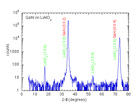
X-ray diffraction was used to determine the precise orientation of the films with respect to the substrate. The measurements were made using a 4-circle diffractometer with monochromatized Cu Kα radiation. For the GaN film, only peaks observed in the θ-2θ scans shown in figure 5 on the substrate normal were the overlapping GaN (0 0 0 2 L ) and LiAlO2( L 0 0) peaks. The LiAlO2(2 L+1 0 0) peaks are forbidden by symmetry, but are present, even if they are very weak. These peaks are also observed on bare γ-LiAlO2 substrates. Measurements of the diffraction from inclined planes confirmed the orientation relationship observed by TEM. An azimuthal scan on the GaN(1

The (rocking curve) scans on unresolved GaN (0 0 0 2) and γ-LiAlO2(2 0 0) peaks for two perpendicular directions are shown in figure 6. Two peaks are clearly resolved, a sharp peak from the substrate (2 0 0) planes (FWHM=0.16°, instrument limited), and a broader peak (FWHM=0.75°) from the GaN (0 0 0 2) peak. θ-2θ scans for the tilted peak revealed a 0.15° shift in 2-θ compared to the peak near the substrate normal. A difference of only 0.05° is expected from the difference between the γ-LiAlO2 (2 0 0) and GaN (0 0 0 2) lattice spacing. These observations confirm the finding from TEM that the film is tilted with respect to the substrate, and give the magnitude of the tilt as 0.56°. Note that the film peak is tilted in only one direction in the substrate a-c plane. To check for possible causes of this broken symmetry, we measured the inclination of the surface normal with respect to the crystallographic a-axis. This was done by observing the precession around the substrate a-axis of a He-Ne laser beam reflected from the surface of the sample during azimuthal rotation. We found that the surface was inclined only slightly, 0.16°, roughly in the substrate a-c plane.

Figure 6. X-ray diffraction rocking curves on GaN (0 0 0 2) and γ-LiAlO2(2 0 0) peaks for rocking in two perpendicular directions. The LiAlO2 peak is limited by the instrument resolution.
Similar measurements were done to check whether the crystallographic tilt was also present in films initiated with AlN. For a GaN film grown on an AlN buffer layer, the tilt was roughly 0.3°. The rocking curve was considerably broader than that of the GaN film grown directly on LiAlO2, 1.26° compared to 0.75°. For a thick AlN layer grown on an LiAlO2, the tilt was roughly 0.7°, with a rocking curve FWHM of 2.3°.
3.3 SIMS
A GaN sample grown on a LiAlO2 substrate was analyzed for Ga and O using secondary ion mass spectroscopy (SIMS) by C. Evans &Assoc. Footnote [c] The film was swabbed with methanol to remove any Ga droplets prior to analysis. O was present at a level of approximately 4×1020 cm−3 in the film. This level of oxygen impurities is a factor of 10 higher than typical for GaN films grown during the same period of time. However, we cannot exclude the possibility that this high impurity background is unrelated to the substrate material.
3.4 Electrical
The Hall effect was measured to determine the carrier concentration and mobility in the film. The van der Pauw geometry was used. The room temperature mobility was 16 cm2/Vs, with a carrier concentration of 5×1019 cm−3. This low mobility indicates a fairly high level of compensation or disorder.
4. Discussion
The orientation relationship that we observe for GaN on LiAlO2, GaN(0 0 0 1)∥LiAlO2(1 0 0), GaN[1 1 -2 0]∥ LiAlO2 [0 0 1], GaN[1
The observed tilt of the films is somewhat surprising. The usual picture of misfit accommodation in epitaxial growth is that the film grows in a strained state until the film is so thick that the built-up strain energy surpasses the threshold for dislocation formation. Dislocations often enter as pairs, or as loops. The microscopic tilt associated with each dislocation averages out, resulting in no net tilt, although the small tilts contribute to the mosaic spread as observed in x-ray diffraction rocking curves.
Flinn and co-workers Reference Flynn[14] have discussed one way that tilt can accommodate lattice mismatch. The “coherent tilt» that they describe, first observed in the spinel/Al2O3 system by Carter and Schmalzried Reference Carter and Schmalzried[15], perfectly accommodates one dimensional mismatch if
Here d f is a film lattice spacing, d s is the substrate lattice spacing and θt is the tilt angle. Note that d f must be smaller than d s (positive misfit). If the misfit is negative, coherent tilt would require a miscut surface. The coherent tilt angle for the GaN on LiAlO2 system is 8.8°, much larger than we observe. In addition, the coherent tilt process cannot explain the tilts we observe for AlN grown on LiAlO2., since the relevant misfit is negative. Another way that a film might be tilted crystallographically with respect to a substrate is by grapho-epitaxy on a miscut substrate. Here the substrate acts as a physical template for epitaxy, but has very weak chemical bonding to the film. The expected tilt is just the miscut angle. Since the tilt we observe is 3 times the miscut, grapho-epitaxy can only partially explain our results. The small miscut may be responsible for the bias of the tilt we observe; although there is a chirality of the crystal along its c axis, it should not be apparent on the (1 0 0) surface.
Another mechanism Reference Nagai[16] Reference Auvray, Baudet and Regreny[17] has been observed to cause very small tilts on miscut substrates. When the film has a larger lattice constant than a miscut substrate, the film tilts to match the step heights on the surface. This is inapplicable to the current system because the step height misfit for c GaN on a LiAlO2 is extremely small.
The amount of tilt that would be obtained if all of the misfit dislocations were oriented so that their tilt components added coherently can be simply computed. It is just
b is the Burgers vector of the dislocation, n is the unit vector normal to the substrate and Λd is the linear density of dislocations. Only the component of the Burgers vector tangent to the substrate surface is effective at relieving misfit, so there is no generic reason for misfit to give rise to tilt. In the case of coherent tilt the Burger's vector is tilted with the film and thus acquires a component tangent to the substrate surface. For the present case, if we choose Burger's vectors distributed between (1/3 [1
Although the observed orientation relationship are not surprising in retrospect, it is still rather surprising that despite the extremely favorable lattice match and structure match there is no tendency at all to form a oriented GaN films on the a plane of LiAlO2. Although GaN typically grows with an (0 0 0 1) habit, it is still surprising that not even a small fraction of the GaN would grow in this orientation. Figure 7a and figure 7b show that the structural mismatch for the c GaN on a LiAlO2 is entirely in the direction normal to the interface. The white circles in figure 7 represent the dangling bonds on these two surfaces. The match is poor. It is possible that at surfaces or in monolayers, these bonds may hybridize to form a more hexagonal BN-like structure. Future work on the surface structure of LiAlO2 and on the structure of GaN surface monolayers may resolve this mystery.

Figure 7a. (1 0 0) surface mesh of γ-LiAlO2. Note that half the atoms of each type have a dangling bond (denoted by the white circles) pointing out of the surface. Li atoms are green, Al atoms are red, O atoms are blue.

Figure 7b. (0 0 0 1) surface mesh of GaN. Note that either all of the gallium atoms or all of the nitrogen atoms, depending on the polarity, have dangling bonds pointing out. Ga atoms are magenta, N atoms are aqua.

Figure 8a. Schematic of a completely incoherent interface with 10% misfit. every half coherence length, the two lattices are exactly out of phase.

Figure 8b. Schematic of an incoherent interface with tilt. Note that the out-of-phase regions are eliminated. This will lower the interface energy in polar crystals.
5. Conclusion
We have observed the orientation relationships of GaN grown on a-plane LiAlO2 substrates. We find that c-oriented GaN and AlN grow with a small tilt in the plane of the nearly lattice matched direction. The magnitude of the tilt is consistent with that required to reduce the interface energy by tilting an incoherent interface. This mechanism for misfit accommodation appears not to have been previously recognized.
There are still a number of unresolved issues. In particular, we have essentially ignored the large misfit along the substrate b direction and its effect on the tilt. Even so, control of the incoherent tilt phenomenon may be a way to improve the materials quality of epitaxial films in a variety of large misfit systems, and it may prove fruitful to apply this understanding to the growth of GaN and AlN on sapphire.
Acknowledgments
The authors would like to thank Bruce Chai of Crystal Photonics, Inc, for supplying the LiAlO2 substrates. ZLW work was supported by the Director, Office of Energy Research, Office of Basic Energy Sciences, Division of Materials Sciences, of the U.S. Department of Energy under Contract No. DE-AC03-76SF00098. She wants to acknowledge W. Swider for excellent TEM sample preparation.