


Introduction
The particular features that make the III-nitrides and SiC attractive for high frequency, high power device applications are their relatively high breakdown voltage, high saturation electron drift velocity, low dielectric constants, and for SiC, high thermal conductivity [Reference Weitzel1-Reference Shenai, Scott and Baliga3].
To the authors’ knowledge, only a few other theoretical studies of the behavior of GaN based FETs have been made [Reference Schwierz, Kittler, Forster and Schipinski4-Reference Farahmand and Brennan7]. The theoretical study of GaN based devices is frustrated to some extent by the paucity of reliable transport parameters. As such, numerical studies using advanced drift diffusion and hydrodynamic simulation tools [Reference Smith and Brennan8] that require extensive parameterization are, at present, challenging. Alternatively, less parameterized models, such as the full band ensemble Monte Carlo technique that can proceed relatively independently of experiment, are presently more suitable for studying transport in GaN and in modeling GaN based devices [Reference F Brennan, Kolnik, Oguzman, Bellotti, Farahmand, Ruden, Wang, Albrecht and Pearton9]. It has been shown that Monte Carlo simulations using an analytical band structure approximation are generally insufficiently detailed to properly describe high field transport dynamics [Reference Fischetti and Laux10]. Inclusion of the full details of the band structure is necessary to provide an accurate accounting of the breakdown properties of a device. For these reasons, we employ a full band ensemble Monte Carlo simulation to examine the relative performance characteristics of wurtzite and zincblende phase GaN MESFETs operated near breakdown. The model is summarized in the next section. In section III, the calculated results are presented and conclusions are drawn in Section IV.
Model Description
The full band Monte Carlo technique relies on the knowledge of fairly well known parameters i.e., lattice constants, energy gaps, phonon energies, dielectric constants, etc. From these quantities a reasonably accurate description of the band structure, impact ionization transition rate and phonon scattering rates can be obtained, enabling study of the basic transport properties of the material and its related devices. The full band Monte Carlo simulator can thus be developed without extensive experimental knowledge of the transport parameters of a material. Though the Monte Carlo model suffers from some basic uncertainties, these mainly being in the details of the deformation potentials and the concomitant high energy scattering rates, it is nonetheless presently the most reliable simulation tool for investigating high field transport.
The full details of our Monte Carlo model have been presented elsewhere [Reference F Brennan, Kolnik, Oguzman, Bellotti, Farahmand, Ruden, Wang, Albrecht and Pearton9]. In addition, the details of how our Monte Carlo model has been merged with a Poisson solver to enable device simulation have also been discussed elsewhere [Reference Farahmand and Brennan6]. For brevity we will not repeat these details here.
This study is comparative in nature. The study is not meant to project the ultimate limits of potential performance of GaN MESFETs. Instead, it is our goal to examine devices with the same geometry and doping concentrations but made using the two different polytypes of GaN, wurtzite and zincblende, to provide some basis of comparison of how the device performance varies, if at all, with choice of polytype. The geometry and doping concentrations for the device structure used in this study are shown in Figure 1. The very small dimensions of the device are chosen mainly to manage the computational demands of the simulator. All of the calculations are made assuming an ambient temperature of 300K. The dopants are assumed to be fully ionized and no doping compensation is present.
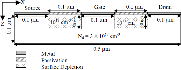
Figure 1. Cross section of the MESFET.
In our previous theoretical studies of the transport properties of the III-nitrides [Reference Kolnik, Oguzman, Brennan, Wang and Ruden11-Reference Oguzman, Kolnik, Brennan, Wang, Fang and Ruden14] we have encountered new physical effects which influence the transport calculations in non-cubic symmetry semiconductors [Reference Brennan, Bellotti, Farahmand, Nilsson, Ruden and Zhang15]. Perhaps the most important effect encountered in modeling non-cubic symmetry semiconductors is that of band intersections. In materials with highly complex band structures, such as wurtzite phase GaN, numerous band intersection points occur. Proper treatment of these points is necessary to render an accurate description of the transport dynamics. We have developed two approaches to treating transport near these points. The first approach is based on the evaluation of the overlap integral of the cell periodic part of the wave function between the initial and possible final states of the intersecting bands. The final state is selected stochastically based on the relative probabilities given by the overlap integrals [Reference Oguzman, Bellotti, Brennan, Kolnik, Wang and Ruden12]. The second approach is based on a velocity continuation test performed at band intersections [Reference Farahmand and Brennan6]. As in the case for the overlap integral test, the final state is selected stochastically but with the difference that the choice is based on the requirement of velocity continuation during the drift. Good agreement between the two models has been observed. It should be noted however that neither one of these techniques definitively describes the transport physics at band intersections. Instead, these approaches are only initial attempts at modeling the effects of band intersections and as such provide only a first order approximation of multiband transport effects. A more complete study of the physics of transport near band intersections is currently underway.
In the present study we adopt the velocity continuation approach for treating band intersection points. Though we currently believe that the overlap integral method is more fundamentally sound, that technique presently requires more computational resources. The device simulator used here, when band intersection effects are neglected as can be done in the zincblende phase GaN calculations, already highly stresses our computational capabilities. Therefore, when band intersection effects must be included, as is necessary in wurtzite phase GaN, computational efficiency becomes of the highest priority. Though we cannot presently be certain as to how accurate the velocity continuation test is, its observed empirical agreement with the overlap integral test gives some confidence that this model is acceptable, at least to first order. In any event, the present limitations of our computational resources precludes doing much else.
Calculated Results
The calculated drain current, Id, versus drain-source voltage, Vds, for gate-source voltages, Vgs, varying from −0.1V to −5.1V in 1V steps for the zincblende phase and the wurtzite phase devices are shown in Figure 2. The Schottky barrier potential height was included in Vgs. For each bias point, the drain current was calculated under two conditions. These were with and without the presence of impact ionization. This was done in order to calculate the breakdown voltage[Reference Farahmand and Brennan7].
Figure 2. Output characteristics for the zincblende phase device (a) and the wurtzite phase device (b). The gate-source voltage, Vgs includes the Schottky barrier height. The drain currents have been calculated with impact ionization (solid lines) and without impact ionization (dashed lines). The ovals show the breakdown locations on the I-V curves.
As it can be observed from Figure 2, the breakdown voltages are significantly higher in the wurtzite phase device than in the zincblende phase device. The higher breakdown voltage of the wurtzite device is attributed to the higher density of electronic states in the wurtzite phase than in the zincblende phase GaN. As a result of the greater electronic density of states, the electrons are, on the average, cooler in the wurtzite phase than in the zincblende phase under the same biasing conditions.
The current-voltage characteristics shown in Figure 2, exhibit a finite slope even at the lowest gate-source voltage reported which is mainly a consequence of the very small gate length examined. The late turn-on observed for the curves with the most negative gate-source voltages is due to the potential barrier under the gate which blocks the source electrons from reaching the drain contact. This potential barrier limits the drain-source current until a sufficiently large drain-source bias is applied, which lifts the barrier to allow an appreciable current flow.
The current gain cutoff frequency, fT was calculated from the following expression,

where gm is the transconductance and Cg is the gate capacitance obtained by the incremental charge partitioning method [16 ]. The calculated gate capacitance was 1.519 pF/cm for the zincblende device and 1.572 pF/cm for the wurtzite device. The calculated maximum cutoff frequency and transconductance for the zincblende device were calculated to be fT = 220 GHz and gm = 210 mS/mm which are higher than the cutoff frequency of fT = 160 GHz, and transconductance of gm = 158 mS/mm predicted for an otherwise equivalent wurtzite device. The higher transconductance and cutoff frequency of the zincblende phase GaN MESFET can be explained as follows. Due to the short device length, the electrons within the device experience velocity overshoot. The velocity overshoot is to first order, proportional to the inverse effective mass. The electrons have a lower effective mass in the zincblende phase than the wurtzite phase and consequently, the electron velocity overshoot in the zincblende phase is higher than that in the wurtzite phase. The higher magnitude of velocity overshoot in the zincblende phase as compared to the wurtzite phase has also been observed by Foutz et al. [Reference Foutz, Eastman, Bhapkar and Shur17]. It is hypothesized that the calculated higher cutoff frequency and transconductance for the zincblende phase device is due to the higher overshoot velocity in zincblende phase GaN material.
Conclusions
In this paper, the first full band comparison of the breakdown and high frequency properties of both zincblende and wurtzite phase GaN MESFETs was presented. The calculations were made using a full band, ensemble Monte Carlo simulation including a numerical formulation of the impact ionization transition rates. It was found that the drain current in both phases of the GaN MESFET increases gradually with increasing drain voltage after the onset of breakdown.
It was further found that the breakdown voltage of the zincblende phase GaN device is less than the breakdown voltage of an otherwise equivalent wurtzite phase device. This is due to the lower density of states in zincblende phase GaN, which results in a warmer electron distribution than in the wurtzite phase GaN under similar field conditions. The higher breakdown voltage of the wurtzite phase device results in higher maximum output power.
The cutoff frequency and transconductance of the zincblende phase device was found to be higher than that of the wurtzite phase device. The difference in the calculated cutoff frequencies was attributed to the higher electron overshoot velocity in the zincblende phase. The maximum transconductance and cutoff frequency were calculated from the Monte Carlo simulation to be 210 mS/mm and 220 GHz for the zincblende phase MESFET, and 158 mS/mm and 160 GHz for the wurtzite phase MESFETs respectively.
It should be noted that due to the basic uncertainties in the band structure, phonon scattering rates, and ionization coefficients, the calculations presented herein serve only as a general guide to the expected performance measures of GaN MESFET devices. It should be further noted that the breakdown properties predicted here rely on previous theoretical estimates of the impact ionization coefficients that have a high degree of uncertainty and have yet to be experimentally verified. Nevertheless, on the basis of these calculations it can be expected that very high frequency performance at high breakdown voltage for GaN based MESFET structures can be obtained. In addition, it is also reasonably certain that a zincblende phase GaN MESFET structure will have a higher cutoff frequency and transconductance than an otherwise identical wurtzite phase GaN MESFET device. On the other hand, the GaN wurtzite phase device will have a higher breakdown voltage than the GaN zincblende phase device.
Acknowledgements
This work was sponsored by the National Science Foundation through grant ECS-9811366. Additional support was received by the Office of Naval Research through contract E21-K09, by the Office of Naval Research through subcontract E21-K69 made to Georgia Tech through the UCSB MURI program. Usage of the Intel Corp. Advanced Platform Computer Cluser at Georgia Tech is gratefully acknowledged.

