Hostname: page-component-586b7cd67f-tf8b9 Total loading time: 0 Render date: 2024-11-30T10:36:27.086Z Has data issue: false hasContentIssue false

Determination of the barrier height of iridium with hydrogen-terminated single crystal diamond

Published online by Cambridge University Press:  12 February 2019
Yan-Feng Wang
Affiliation:
Institute of Wide Band Gap Semiconductors, Shaanxi Key Lab of Information Photonic Technique, Xi'an Jiaotong University, Xi'an 710049, Shaanxi Province, China
Wei Wang
Affiliation:
Institute of Wide Band Gap Semiconductors, Shaanxi Key Lab of Information Photonic Technique, Xi'an Jiaotong University, Xi'an 710049, Shaanxi Province, China
Xiaohui Chang
Affiliation:
Institute of Wide Band Gap Semiconductors, Shaanxi Key Lab of Information Photonic Technique, Xi'an Jiaotong University, Xi'an 710049, Shaanxi Province, China
Juan Wang
Affiliation:
Institute of Wide Band Gap Semiconductors, Shaanxi Key Lab of Information Photonic Technique, Xi'an Jiaotong University, Xi'an 710049, Shaanxi Province, China
Jiao Fu
Affiliation:
Institute of Wide Band Gap Semiconductors, Shaanxi Key Lab of Information Photonic Technique, Xi'an Jiaotong University, Xi'an 710049, Shaanxi Province, China
Tianfei Zhu
Affiliation:
Institute of Wide Band Gap Semiconductors, Shaanxi Key Lab of Information Photonic Technique, Xi'an Jiaotong University, Xi'an 710049, Shaanxi Province, China
Zongchen Liu
Affiliation:
Institute of Wide Band Gap Semiconductors, Shaanxi Key Lab of Information Photonic Technique, Xi'an Jiaotong University, Xi'an 710049, Shaanxi Province, China
Yan Liang
Affiliation:
Institute of Wide Band Gap Semiconductors, Shaanxi Key Lab of Information Photonic Technique, Xi'an Jiaotong University, Xi'an 710049, Shaanxi Province, China
Dan Zhao
Affiliation:
Institute of Wide Band Gap Semiconductors, Shaanxi Key Lab of Information Photonic Technique, Xi'an Jiaotong University, Xi'an 710049, Shaanxi Province, China
Zhangcheng Liu
Affiliation:
Institute of Wide Band Gap Semiconductors, Shaanxi Key Lab of Information Photonic Technique, Xi'an Jiaotong University, Xi'an 710049, Shaanxi Province, China
Minghui Zhang
Affiliation:
Institute of Wide Band Gap Semiconductors, Shaanxi Key Lab of Information Photonic Technique, Xi'an Jiaotong University, Xi'an 710049, Shaanxi Province, China
Kaiyue Wang
Affiliation:
Institute of Wide Band Gap Semiconductors, Shaanxi Key Lab of Information Photonic Technique, Xi'an Jiaotong University, Xi'an 710049, Shaanxi Province, China School of Materials Science and Engineering, Taiyuan University of Science and Technology, Taiyuan 030024, Shanxi Province, China
Hong-Xing Wang*
Affiliation:
Institute of Wide Band Gap Semiconductors, Shaanxi Key Lab of Information Photonic Technique, Xi'an Jiaotong University, Xi'an 710049, Shaanxi Province, China
Ruozheng Wang
Affiliation:
Institute of Wide Band Gap Semiconductors, Shaanxi Key Lab of Information Photonic Technique, Xi'an Jiaotong University, Xi'an 710049, Shaanxi Province, China
*
Address all correspondence to Hong-Xing Wang at hxwangcn@mail.xjtu.edu.cn
Get access

Abstract

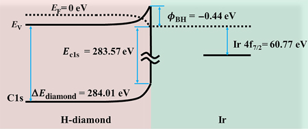
Direct determination of barrier height (ΦBH) value between Ir and single crystal (001) hydrogen-terminated diamond with lightly boron doped has been performed using x-ray photoelectron spectroscopy technique. 70 nm Ir islands were formed on hydrogen-terminated diamond surface using anodic aluminum oxide. The ΦBH value for Ir/hydrogen-terminated diamond was −0.43 ± 0.14 eV, indicating that Ir was a suitable metal for ohmic contact with hydrogen-terminated diamond. The band diagram of Ir/hydrogen-terminated diamond was obtained. The experimental ΦBH was compared with the theoretical ΦBH in this work.

Type
Research Letters
Copyright
Copyright © Materials Research Society 2019 

Access options

Get access to the full version of this content by using one of the access options below. (Log in options will check for institutional or personal access. Content may require purchase if you do not have access.)

References

1.Imanishi, S., Horikawa, K., Oi, N., Okubo, S., Kageura, T., Hiraiwa, A., and Kawarada, H.: 3.8 W/mm power density for ALD Al2O3-based two-dimensional hole gas diamond MOSFET operating at saturation velocity. IEEE Electron Device Lett. 1, 99102 (2018).Google Scholar
2.Liu, J., Ohsato, H., Liao, M., Imura, M., Watanabe, E., and Koide, Y.: Logic circuits with hydrogenated diamond field-effect transistors. IEEE Electron Device Lett. 38, 992–925 (2017).Google Scholar
3.Wang, Y-F., Chang, X., Zhang, X., Fu, J., Fan, S., Bua, R., Zhang, J., Wang, W., Wang, H-X., and Wang, J.: Normally-off hydrogen-terminated diamond field-effect transistor with Al2O3 dielectric layer formed by thermal oxidation of Al. Diam. Relat. Mater. 81, 113117 (2018).Google Scholar
4.Wang, Y-F., Chang, X., Li, S., Zhao, D., Shao, G., Zhu, T., Fu, J., Zhang, P., Chen, X., Li, F., Liu, Z., Fan, S., Bu, R., Wen, F., Zhang, J., Wang, W., and Wang, H-X.: Ohmic contact between iridium film and hydrogen-terminated single crystal diamond. Sci. Rep. 7, 12157 (2017).Google Scholar
5.Verona, C., Arciprete, F., Foffi, M., Limiti, E., Marinelli, M., Placidi, E., Prestopino, G., and Verona Rinati, G.: Influence of surface crystal-orientation on transfer doping of V2O5/H-terminated diamond. Appl. Phys. Lett. 112, 181602 (2018).Google Scholar
6.Kitabayashi, Y., Kudo, T., Tsuboi, H., Yamada, T., Xu, D., Shibata, M., Matsumura, D., Hayashi, Y., Syamsul, M., Inaba, M., Hiraiwa, A., and Kawarada, H.: Normally-Off C–H Diamond MOSFETs With Partial C–O Channel Achieving 2-kV Breakdown Voltage. IEEE Electron Device Lett. 38, 363366 (2017).Google Scholar
7.Wang, W., Fu, K., Hu, C., Li, F.N., Liu, Z.C., Li, S.Y., Lin, F., Fu, J., Wang, J.J., and Wang, H.X.: Diamond based field-effect transistors with SiNx and ZrO2 double dielectric layers. Diam. Relat. Mater. 69, 237240 (2016).Google Scholar
8.Syamsul, M., Oi, N., Okubo, S., Kageura, T., and Kawarada, H.: Heteroepitaxial diamond field-effect transistor for high voltage applications. IEEE Electron Device Lett. 39, 5154 (2018).Google Scholar
9.Huang, B., Bai, X., Lam, S.K., and Tsang, K.K.: Diamond FinFET without hydrogen termination. Sci. Rep. 8, 3063 (2018).Google Scholar
10.Crawford, K.G., Qi, D., McGlynn, J., Ivanov, T.G., Shah, P.B., Weil, J., Tallaire, A., Ganin, A.Y., and Moran, D.A.J.: Thermally stable, high performance transfer doping of diamond using transition metal oxides. Sci. Rep. 8, 3342 (2018).Google Scholar
11.Imura, M., Hayakawa, R., Ohsato, H., Watanabe, E., Tsuya, D., Nagata, T., Liao, M., Koide, Y., Yamamoto, J-I., Ban, K., Iwaya, M., and Amano, H.: Development of AlN/diamond heterojunction field effect transistors. Diam. Relat. Mater. 124, 206209 (2012).Google Scholar
12.Werner, M., Job, R., Denisenko, A., Zaitsev, A., Fahrner, W.R., Johnston, C., Chalker, P.R., and Buckley-Golder, I.M.: How to fabricate low-resistance metal-diamond contacts. Diam. Relat. Mater. 5, 723727 (1996).Google Scholar
13.Wang, W., Hu, C., Li, F.N., Li, S.Y., Liu, Z.C., Wang, F., Fu, J., and Wang, H.X.: Palladium Ohmic contact on hydrogen-terminated single crystal diamond film. Diam. Relat. Mater. 63, 175179 (2016).Google Scholar
14.Li, F.N., Liu, J.W., Zhang, J.W., Wang, X.L., Wang, W., Liu, Z.C., and Wang, H.X.: Measurement of barrier height of Pd on diamond (100) surface by X-ray photoelectron spectroscopy. Appl. Surf. Sci. 370, 496500 (2016).Google Scholar
15.Kono, S., Teraji, T., Kodama, H., Ichikawa, K., Ohnishi, S., and Sawabe, A.: Direct determination of the barrier height of Ti-based ohmic contact on p-type diamond (001). Diam. Relat. Mater. 60, 117122 (2015).Google Scholar
16.Yokoba, M., Koide, Yasuo, Otsuki, A., Ako, F., Oku, T., and Murakami, M.: Carrier transport mechanism of Ohmic contact to p-type diamond. J. Appl. Phys. 81, 6815 (1997).Google Scholar
17.Koide, Y., Yokoba, M., Otsuki, A., Ako, F., Oku, T., and Murakami, M.: Carrier transport mechanisms through the metal p-type diamond semiconductor interface. Diam. Relat. Mater. 6, 847851 (1997).Google Scholar
18.Kono, S., Kodama, H., Ichikawa, K., Yoshikawa, T., Abukawa, T., and Sawabe, A.: Electron spectro-microscopic determination of barrier height and spatial distribution of Au and Ag Schottky junctions on boron-doped diamond (001). Jpn. J. Appl. Phys. 53, 05FP03 (2014).Google Scholar
19.Kono, S., Teraji, T., Takeuchi, D., Ogura, M., Kodama, H., and Sawabe, A.: Direct determination of the barrier height of Au ohmic-contact on a hydrogen-terminated diamond (001) surface. Diam. Relat. Mater. 73, 182189 (2017).Google Scholar
20.Freakley, S.J., Ruiz-Esquius, J., and Morgan, D.J.: The X-ray photoelectron spectra of Ir, IrO2 and IrCl3 revisited. Surf. Interface Anal. 49, 8 (2017).Google Scholar
21.Kraut, E.A., Grant, R.W., Waldrop, J.R., and Kowalczyk, S.P.: Precise determination of the valence-band edge in X-ray photoemission spectra application to measurement of semiconductor interface potentials. Phys. Rev. Lett. 44, 16201623 (1980).Google Scholar
22.Tung, R.T.: Recent advances in Schottky barrier concepts. Mater. Sci. Eng., R 35, 1138 (2001).Google Scholar