Skip to main content Accessibility help
×
Hostname: page-component-6d856f89d9-jhxnr Total loading time: 0 Render date: 2024-07-16T04:57:14.532Z Has data issue: false hasContentIssue false

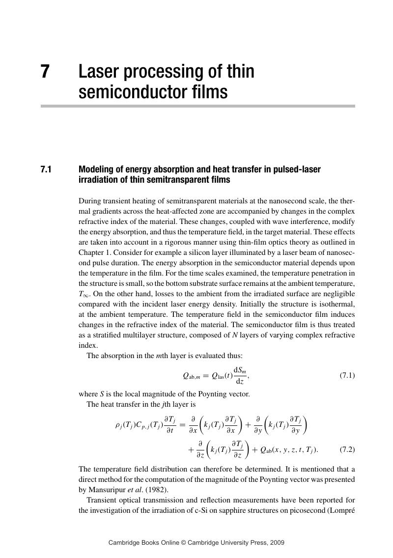
7 - Laser processing of thin semiconductor films

Published online by Cambridge University Press:  04 December 2009

Costas P. Grigoropoulos
Affiliation:
University of California, Berkeley
Get access

Summary

Image of the first page of this content. For PDF version, please use the ‘Save PDF’ preceeding this image.'
Type
Chapter
Information
Transport in Laser Microfabrication
Fundamentals and Applications
, pp. 202 - 239
Publisher: Cambridge University Press
Print publication year: 2009

Access options

Get access to the full version of this content by using one of the access options below. (Log in options will check for institutional or personal access. Content may require purchase if you do not have access.)

References

Aichmayr, G., Toet, D., Mulato, M.et al., 1999, “Dynamics of Lateral Grain Growth during the Laser Interference Crystallization of a-Si,” J. Appl. Phys.,85, 4010–4023.CrossRefGoogle Scholar
Anderson, R. J., 1988, “A Method to Calculate the Laser Heating of Layered Structures,” J. Appl. Phys.,64, 6639–6647.CrossRefGoogle Scholar
Biegelsen, D. K., Fennell, L. E., and Zesch, J. C., 1984, “Origin of Oriented Crystal Growth of Radiantly Melted Silicon on SiO2,” Appl. Phys. Lett.,45, 546–548.CrossRefGoogle Scholar
Bucksbaum, P. H., and Bokor, J., 1984, “Rapid Melting and Regrowth Velocities in Silicon Heated by Ultraviolet Picosecond Laser Pulses,” Phys. Rev. Lett.,53, 182–187.CrossRefGoogle Scholar
Burgener, M. L., and Reedy, R. E., 1982, “Temperature Distributions Produced in a Two Layer Structure by a Scanning CW Laser or Electron Beam,” J. Appl. Phys.,53, 4357–4363.CrossRefGoogle Scholar
Celler, G. K., 1983, “Laser Crystallization of Thin Si Films on Amorphous Insulating Substrates,” J. Cryst. Growth,63, 429–447.CrossRefGoogle Scholar
Chen, S. C., and Grigoropoulos, C. P., 1997, “Non-contact Nanosecond-Time-Resolution Temperature Measurement and Evaluation of Thermal Properties in Excimer Laser Heating of Ni–P Disk Substrates,” Appl. Phys. Lett.,71, 3191–3193.CrossRefGoogle Scholar
Deutsch, T. F., Ehrlich, D. J., Rathman, D. D., Silversmith, D. J., and Osgood, R. M. Jr., 1981, “Electrical Properties of Laser Chemically Doped Silicon,” Appl. Phys. Lett.,39, 825–827.CrossRefGoogle Scholar
DeWitt, D. P., and Rondeau, R. E., 1989, “Measurement of Surface Temperatures and Spectral Emissivities During Laser Irradiance,” J. Thermophys.,3, 153–159.CrossRefGoogle Scholar
Dworshack, K., Sipe, J. E., and Driel, H. M., 1990, “Solid-Melt Patterns Induced on Silicon by a Continuous Laser Beam at Nonnormal Incidence,” J. Opt. Soc. Am. B,7, 981–989.CrossRefGoogle Scholar
Ehlrich, D. J., Brueck, S. R. J., and Tsao, J. Y., 1983, “Surface Electromagnetic Waves in Laser Materials Interactions,” Proc. Mater. Res. Soc.,13, 191–196.Google Scholar
Fauchet, P. M., and Siegman, A. E., 1982, “Surface Ripples on Silicon and Gallium Arsenide under Picosecond Laser Illumination,” Appl. Phys. Lett.,40, 824–826.CrossRefGoogle Scholar
Fan, D., Huang, J., and Jaccodine, R. J., 1987, “Enhanced Tail Diffusion of Ion Implanted Boron in Silicon,” Appl. Phys. Lett.,50, 1745–1747.CrossRefGoogle Scholar
Fan, J. C. C., Tsaur, B.-Y., and Geis, M. W., 1983, “Graphite-Strip Heater Zone-Melting Recrystallization of Si Films,” J. Cryst. Growth,63, 453–483.CrossRefGoogle Scholar
Fisher, J. C., Hollomon, J. H., and Turnbull, D., 1948, “Nucleation,” J. Appl. Phys.,19, 775–784.CrossRefGoogle Scholar
Galvin, G. J., Thompson, M. O., Mayer, J. W.et al., 1982, “Measurement of the Velocity of the Crystal–Liquid Interface in Pulsed Laser Annealing of Si,” Phys. Rev. Lett.,48, 33–36.CrossRefGoogle Scholar
Giust, G. K., and Sigmon, T. W., 1997, “Self-Aligned Aluminum Top-Gate Polysilicon Thin-Film Transistors Fabricated Using Laser Recrystallization and Gas-Immersion Laser Doping,” IEEE Electron Device Lett.,18, 394–396.CrossRefGoogle Scholar
Glazov, V. M., Chizhevskays, S. N., and Glagoleva, N. N., 1969, Liquid Semiconductors, New York, Plenum.CrossRefGoogle Scholar
Grigoropoulos, C. P., Buckholz, R. H., and Domoto, G. A., 1986, “A Heat Transfer Algorithm for the Laser-Induced Melting and Recrystallization of Thin Silicon Layers,” J. Appl. Phys.,60, 2304–2309.CrossRefGoogle Scholar
Grigoropoulos, C. P., Buckholz, R. H., and Domoto, G. A., 1987a, “Stability of Silicon Phase Boundaries,” J. Appl. Phys.,62, 474–479.CrossRefGoogle Scholar
Grigoropoulos, C. P., Buckholz, R. H., and Domoto, G. A., 1987b, “A Thermal Instability in the Laser Driven Melting and Recrystallization of Thin Silicon Films on Glass Substrates,” J. Heat Transfer,109, 841–847.CrossRefGoogle Scholar
Grigoropoulos, C. P., Buckholz, R. H., and Domoto, G. A., 1988, “An Experimental Study on Laser Annealing of Thin Silicon Layers,” J. Heat Transfer,110, 416–423.CrossRefGoogle Scholar
Grigoropoulos, C. P., and Dutcher, W. E., 1992, “Moving Front Fixing in Thin Film Laser Annealing,” J. Heat Transfer,114, 271–277.CrossRefGoogle Scholar
Grigoropoulos, C. P., Dutcher, W. E., and Emery, A. F., 1991a, “Experimental and Computational Analysis of CW Argon Laser Melting of Thin Silicon FilmsJ. Heat Transfer,113, 21–29.CrossRefGoogle Scholar
Grigoropoulos, C. P., Dutcher, W. E., and Barclay, K. E, 1991b, “Radiative Phenomena in CW Laser Annealing,” J. Heat Transfer,113, 657–662.CrossRefGoogle Scholar
Grigoropoulos, C. P., Emery, A. F., and Wipf, E., 1990, “Heat Transfer in Thin Silicon Films by Laser Line Sources,” Int. J. Heat Mass Transfer,33, 797–803.CrossRefGoogle Scholar
Grigoropoulos, C. P., Rostami, A. A., Xu, X., Taylor, S. L., and Park, H. K., 1993, “Localized Transient Surface Reflectivity Measurements and Comparison to Heat Transfer Modeling in Thin Film Laser Annealing,” Int. J. Heat Mass Transfer,36, 1219–1229.CrossRefGoogle Scholar
Hatano, M., Moon, S., Lee, M., and Grigoropoulos, C. P., 2000, “Excimer Laser-Induced Temperature Field in Melting and Resolidification of Silicon Thin Films,” J. Appl. Phys.,87, 36–43.CrossRefGoogle Scholar
Hawkins, W. G., and Biegelsen, D. K., 1983, “Origin of Lamellae in Radiatively Melted Silicon Films,” Appl. Phys. Lett.,42, 358–360.CrossRefGoogle Scholar
Herlach, D. M., 1994, “Non-equilibrium Solidification of Undercooled Metallic Melts,” Mater. Sci. Eng.,R12, 177–272.CrossRefGoogle Scholar
Im, J. S., Crowder, M. A., Sposili, R. S.et al., 1999, “Controlled Super-Lateral Growth of Si Films for Microstructural Manipulation and Optimization,” Phys. Status Solidi (a),166, 603–617.3.0.CO;2-0>CrossRefGoogle Scholar
Im, J. S., Gupta, V. V., and Crowder, M. A., 1998, “On Determining the Relevance of Athermal Nucleation in Rapidly Quenched Liquids,” Appl. Phys. Lett.,72, 662–664.CrossRefGoogle Scholar
Im, J. S., Kim, H. J., and Thompson, M. O., 1993, “Phase Transformation Mechanisms Involved in Excimer Laser Crystallization of Amorphous Silicon Films,” Appl. Phys. Lett.,63, 1969–1971.CrossRefGoogle Scholar
Im, J. S., and Sposili, R. S., 1996, “Crystalline Si Films for Integrated Active-Matrix Liquid-Crystal Displays,” Mater. Res. Bull.,21, 39–48.CrossRefGoogle Scholar
Im, J. S., Sposili, R. S., and Crowder, M. A., 1997, “Single-Crystal Si Films for Thin-Film Transistor Devices,” Appl. Phys. Lett.,70, 3434–3436.CrossRefGoogle Scholar
Ishihara, R., and Matsumura, M., 1997, “Excimer-Laser-Produced Single-Crystal Silicon Thin-Film Transistors,” Jap. J. Appl. Phys.,36, 6167–6170.CrossRefGoogle Scholar
Ishikawa, K., Ozawa, M., Ho, C.-H., and Matsumura, M., 1998, “Excimer-Laser-Induced Lateral Growth of Silicon Thin-Films,” Jap. J. Appl. Phys.,37, 731–736.CrossRefGoogle Scholar
Jackson, K. A., and Kurtze, D. A., 1985, “Instability in Radiatively Melted Silicon Films,” J. Cryst. Growt.,71, 385–390.CrossRefGoogle Scholar
Jellison, G. E. Jr., Lowndes, D. H., Mashburn, D. N., and Wood, R. F., 1986, Time-Resolved Reflectivity Measurements of Silicon and Germanium Using a Pulsed Excimer KrF Laser Heating Beam,” Phys. Rev. B,34, 2407–2417.CrossRefGoogle ScholarPubMed
Jellison, G. E. Jr., Lowndes, D. H., and Wood, R. F., 1983, “A Detailed Examination of Time-Resolved Pulsed Raman Temperature Measurements of Laser Annealed Silicon,” Proc. Mater. Res. Soc.,13, 35–40.CrossRefGoogle Scholar
Kant, R., and Deckert, K. L., 1991, “Laser Induced Heating of a Multilayered Medium Resting on a Half-Space. Part II. – Moving Source,” J. Heat Transfer,113, 12–20.CrossRefGoogle Scholar
Kawamura, S., Sakurai, J., Nakano, M., and Takagi, M., 1982, “Recrystallization of Si on Amorphous Substrates by Doughnut-Shaped CW Ar Laser Beam,” Appl. Phys. Lett.,40, 394–397.CrossRefGoogle Scholar
Kim, H. J., and Im, J. S., 1996a, “Optimization and Transformation Analysis of Grain-Boundary-Location-Controlled Si Films,” Proc. Mater. Res. Soc.,697, 401–406.Google Scholar
Kim, H. J., and Im, J. S., 1996b, “New Excimer-Laser-Crystallization Method for Producing Large-Grained and Grain Boundary-Location-Controlled Si Films for Thin Film Transistors,” Appl. Phys. Lett.,68, 1513–1517.CrossRefGoogle Scholar
Kluge, M. D., and Ray, J. R., 1989, “Velocity versus Temperature Relation for Solidification and Melting of Silicon: A Molecular-Dynamics Study,” Phys. Rev. B,39, 1738–1746.CrossRefGoogle ScholarPubMed
Knapp, J. A., and Picraux, S. T., 1983, “Growth of Si on Insulator Using Electron Beams,” J. Cryst. Growth,63, 445–452.CrossRefGoogle Scholar
Kodas, T. T., Baum, T. H., and Comita, P. B., 1987, “Surface Temperature Rise in Multilayered Solids Induced by a Focused Laser Beam,” J. Appl. Phys.,61, 2749–2753.CrossRefGoogle Scholar
Kodera, H., 1963, “Diffusion Coefficients of Impurities in Silicon Melt,” Jap. J. Appl. Phys.,2, 212–219.CrossRefGoogle Scholar
Kraus, H. G., 1987, “Optical Spectral Radiometric/Laser Reflectance Method for Noninvasive Measurement of Weld Pool Surface Temperatures,” Opt. Eng.,26, 1183–1190.CrossRefGoogle Scholar
Lee, M., Moon, S., and Grigoropoulos, C. P., 2001a, “In-situ Visualization of Interface Dynamics during the Double Laser Recrystallization of Amorphous Silicon Thin Films,” J. Cryst. Growth,226, 8–12.CrossRefGoogle Scholar
Lee, M., Moon, S., and Grigoropoulos, C. P., 2001b, “Ultra-Large Lateral Grain Growth by Double Laser Recrystallization of a-Si Films,” Appl. Phys. A,73, 317–322.CrossRefGoogle Scholar
Lee, M., Moon, S., Hatano, M., and Grigoropoulos, C. P., 2000, “Relationship between Fluence Gradient and Lateral Grain Growth in Spatially Controlled Excimer Laser Crystallization of Amorphous Silicon Films,” J. Appl. Phys.,88, 4994–4999.CrossRefGoogle Scholar
Lemons, R. A., and Bosch, M. A., 1982, “Microscopy of Si Films During Laser Melting,” Appl. Phys. Lett.,40, 703–707.CrossRefGoogle Scholar
Leonard, J. P., and Im, J. S., 2001, “Stochastic Modeling of Solid Nucleation in Supercooled Liquids,” Appl. Phys. Lett.,78, 3454–3456.CrossRefGoogle Scholar
Liu, T. M., and Oldham, W. G., 1983, “Channeling Effect of Low Energy Boron Implant in (100) Silicon,” IEEE Electron. Device Lett.,4, 59–62.CrossRefGoogle Scholar
Lompré, L. A., Liu, J. M., Kurz, H., and Bloembergen, N., 1983, “Time-Resolved Temperature Measurement of Picosecond Laser Irradiated Silicon,” Appl. Phys. Lett.,43, 168–170.CrossRefGoogle Scholar
Mansuripur, M., Connell, G. A. N., and Goodman, J. W., 1982, “Laser-Induced Local Heating of Multilayers,” Appl. Opt.,21, 1106–1117.CrossRefGoogle ScholarPubMed
Miaoulis, I. N., and Mikic, B. B., 1986, “Heat Source Power Requirements for High-Quality Recrystallization of Thin Silicon Films for Electronic Devices,” J. Appl. Phys.,59, 1658–1666.CrossRefGoogle Scholar
Moon, S.-J., Lee, M., and Grigoropoulos, C. P., 2002, “Heat Transfer and Phase Transformations in Laser Annealing of Thin Si Films,” J. Heat Transfer,124, 253–264.CrossRefGoogle Scholar
Moon, S., Lee, M., Hatano, M., and Grigoropoulos, C. P., 2000, “Interpretation of Optical Diagnostics for the Analysis of Laser Crystallization of Amorphous Silicon Films,” Micro. Thermoph. Eng.,4, 25–38.Google Scholar
Mullins, W. W., and Sekerka, R. F., 1964, “Stability of a Planar Interface During Solidification of a Dilute Binary Alloy,” J. Appl. Phys.,35, 444–451.CrossRefGoogle Scholar
Murakami, K., Eryu, O., Takita, K., and Masuda, K., 1987, “Explosive Crystallization Starting from an Amorphous-Silicon Surface Region during Long-Pulse Laser Irradiation,” Phys. Rev. Lett.,59, 2203–2206.CrossRefGoogle Scholar
Nemanich, R. J., Biegelsen, D. K., and Hawkins, W. G., 1983, “Aligned, Coexisting Liquid and Solid Regions in Pulsed and CW Laser-Annealed Si,” Phys. Rev. B,27, 7817–7819.CrossRefGoogle Scholar
Ng, K. K., and Lynch, W. T., 1987, “The Impact of Intrinsic Series Resistance on MOSFET Scaling,” IEEE Trans. Electron Devices,34, 503–511.CrossRefGoogle Scholar
Nissim, Y. I., Lietoila, A., Gold, R. B., and Gibbons, J. F., 1980, “Temperature Distributions Produced in Semiconductors by a Scanning Elliptical or Circular CW Laser Beam,” J. Appl. Phys.,51, 274–279.CrossRefGoogle Scholar
Oh, C.-H., Ozawa, M., and Matsumura, M., 1998, “A Novel Phase-Modulated Excimer-Laser Crystallization Method of Silicon Thin Films,” Jap. J. Appl. Phys.,37-Part 2, L492–L497.CrossRefGoogle Scholar
Park, H. K., Xu, X., Grigoropoulos, C. P.et al., 1992, “Temporal Profile of Optical Transmission Probe for Pulsed Laser Irradiation of Amorphous Silicon Films, Appl. Phys. Lett.,61, 749–751.CrossRefGoogle Scholar
Preston, J. S., Sipe, J. E., and Driel, H. M., 1986a, “Phase Diagram of Laser Induced Melt Morphologies on Silicon,” Proc. Mater. Res. Soc.,51, 137–142.CrossRefGoogle Scholar
Preston, J. S., Sipe, J. E., and Driel, H. M., 1986b, “Laser-Induced Morphological Phase-Transitions on Silicon Surfaces,” J. Opt. Soc. Am. B, 3, 156–157.Google Scholar
Preston, J. S., Sipe, J. E., Driel, H. M., and Luscombe, J., 1989, “Optical Absorption in Metallic–Dielectric Microstructures, Phys. Rev. B,40, 3931–3941.CrossRefGoogle ScholarPubMed
Preston, J. S., Driel, H. M., and Sipe, J. E., 1987, “Order–Disorder Transitions in the Melt Morphology of Laser-Irradiated Silicon,” Phys. Rev. Lett.,58, 69–72.CrossRefGoogle ScholarPubMed
Preston, J. S., Driel, H. M., and Sipe, J. E., 1989b, “Pattern Formation during Laser Melting of Silicon,” Phys. Rev. B,40, 3942–3953.CrossRefGoogle ScholarPubMed
Sands, T., Washburn, J., Gronsky, R.et al., 1984, “Near-Surface Defects Formed during Rapid Thermal Annealing of Preamorphized and BF+2-Implanted Silicon,” Appl. Phys. Lett.,45, 982–987.CrossRefGoogle Scholar
Sedwick, T. O., 1981, “A Simple Optical Pyrometer for In-situ Temperature Measurement during CW Laser Annealing”, Proc. Mater. Res. Soc.,1, 147–153.CrossRefGoogle Scholar
Siegel, R., and Howell, J. R., 1992, Thermal Radiation Heat Transfer, 3rd edn, Washington D.C., Taylor and Francis.Google Scholar
Sipe, J. E., Young, J. F., Preston, J. S., and Driel, H. M., 1983, “Laser-Induced Periodic Surface Structure. I. Theory,” Phys. Rev. B,27, 1141–1157.CrossRefGoogle Scholar
Slack, G., 1964, “Thermal Conductivity of Pure and Impure Silicon, Silicon Carbide and Diamond,” J. Appl. Phys.,35, 3460–3466.CrossRefGoogle Scholar
Slaoui, A., Foulon, F., and Siffert, P., 1990, “Excimer Laser Induced Doping of Phosphorus into Silicon,” J. Appl. Phys.,67, 6197–6201.CrossRefGoogle Scholar
Sposili, R. S., and Im, J. S., 1996, “Sequential Lateral Solidification of Thin Silicon Films on SiO2,” Appl. Phys. Lett.,69, 2864–2866.CrossRefGoogle Scholar
Stich, I., Car, R., and Parrinnello, M., 1989, “Bonding and Disorder in Liquid Silicon,” Phys. Rev. Lett.,63, 2240–2243.CrossRefGoogle ScholarPubMed
Stiffler, S. R., and Thompson, M. O., 1988, “Supercooling and Nucleation of Silicon after Laser Melting,” Phys. Rev. Lett.,60, 2519–2522.CrossRefGoogle ScholarPubMed
Stolk, P. A., Polman, A., and Sinke, W. C., 1993, “Experimental Test of Kinetic Theories for Heterogeneous Freezing in Silicon,” Phys. Rev. B,47, 5–13.CrossRefGoogle ScholarPubMed
Stultz, T. J., and Gibbons, J. F., 1981, “The Use of Beam Shaping to Achieve Large-Grain CW Laser-Recrystallized Polysilicon on Amorphous Substrates,” Appl. Phys. Lett.,39, 498–500.CrossRefGoogle Scholar
Tai, Y. C., Mastrangelo, C. H. and Muller, R. S., 1988, “Thermal Conductivity of Heavily Doped Low-Pressure Chemical Vapor Deposited Polycrystalline Silicon Films,” J. Appl. Phys.,63, 1442–1447.CrossRefGoogle Scholar
Thompson, M. O., Galvin, G. J., Mayer, J. W.et al., 1984, “Melting Temperature and Explosive Crystallization of Amorphous Silicon during Pulsed Laser Irradiation,” Phys. Rev. Lett.,52, 2360–2363.CrossRefGoogle Scholar
Usami, A., Ando, M., Tsunekane, M. and Wada, T., 1992, “Shallow-Junction Formation on Silicon by Rapid Thermal Diffusion of Impurities from a Spin-on-Source,” IEEE Trans. Electron Devices,39, 105–110.CrossRefGoogle Scholar
Weiner, K. H., Carey, P. G., McCarthy, A. M., and Sigmon, T. W., 1993, “An Excimer-Laser-Based Nanosecond Thermal Diffusion Technique for Ultra-Shallow pn Junction Fabrication,” Microelectron Eng.,20, 107–130.CrossRefGoogle Scholar
Wolf, S. and Tauber, R. N., 1986, Silicon Processing for the VLSI Era, Vol. 1, New York, Lattice Press, p. 251.Google Scholar
Wood, R. F., and Geist, G. A., 1986a, “Theoretical Analysis of Explosively Propagating Molten Layers in Pulsed-Laser-Irradiated a-Si,” Phys. Rev. Lett.,57, 873–876.CrossRefGoogle ScholarPubMed
Wood, R. F., and Geist, G. A., 1986b, “Modeling of Nonequilibrium Melting and Solidification in Laser-Irradiated Materials,” Phys. Rev. B,34, 2606–2620.CrossRefGoogle ScholarPubMed
Wood, R. F., Geist, G. A., and Liu, C. L., 1996, “Two-Dimensional Modeling of Pulsed Laser-Irradiated a-Si and Other Materials,” Phys. Rev. B,53, 15863–15870.CrossRefGoogle ScholarPubMed
Xu, X., Taylor, S. L., Park, H. K., and Grigoropoulos, C. P., 1993, “Transient Heating and Melting Transformations in Argon-Ion Laser Irradiation of Polysilicon Films,” J. Appl. Phys.,73, 8088–8096.CrossRefGoogle Scholar
Xu, L., Grigoropoulos, C. P., and King, T.-J., 2006, “High Performance Thin Silicon Film Transistors Fabricated by Double Laser Crystallization,” J. Appl. Phys.,99, 034508.CrossRefGoogle Scholar
Young, J. F., Preston, J. S., Driel, H. M., and Sipe, J. E., 1983, “Laser-Induced Periodic Surface Structure. II. Experiments on Ge, Si, Al, and Brass,” Phys. Rev. B,27, 1155–1172.CrossRefGoogle Scholar
Zhang, X., Ho, J.-R., and Grigoropoulos, C. P., 1996, “Ultrashallow p+-Junction Formation in Silicon by Excimer Laser Doping – A Heat and Mass Transfer Perspective,” Int. J. Heat Mass Transfer,39, 3835–3844.CrossRefGoogle Scholar

Save book to Kindle

To save this book to your Kindle, first ensure coreplatform@cambridge.org is added to your Approved Personal Document E-mail List under your Personal Document Settings on the Manage Your Content and Devices page of your Amazon account. Then enter the ‘name’ part of your Kindle email address below. Find out more about saving to your Kindle.

Note you can select to save to either the @free.kindle.com or @kindle.com variations. ‘@free.kindle.com’ emails are free but can only be saved to your device when it is connected to wi-fi. ‘@kindle.com’ emails can be delivered even when you are not connected to wi-fi, but note that service fees apply.

Find out more about the Kindle Personal Document Service.

Available formats
×

Save book to Dropbox

To save content items to your account, please confirm that you agree to abide by our usage policies. If this is the first time you use this feature, you will be asked to authorise Cambridge Core to connect with your account. Find out more about saving content to Dropbox.

Available formats
×

Save book to Google Drive

To save content items to your account, please confirm that you agree to abide by our usage policies. If this is the first time you use this feature, you will be asked to authorise Cambridge Core to connect with your account. Find out more about saving content to Google Drive.

Available formats
×