Skip to main content Accessibility help
×
Hostname: page-component-77c89778f8-rkxrd Total loading time: 0 Render date: 2024-07-20T18:14:42.613Z Has data issue: false hasContentIssue false

3 - Optical Materials And Waveguides

from Part II - Passive Components

Published online by Cambridge University Press:  05 April 2015

Lukas Chrostowski
Affiliation:
University of British Columbia, Vancouver
Michael Hochberg
Affiliation:
Coriant Advanced Technology Group
Get access

Summary

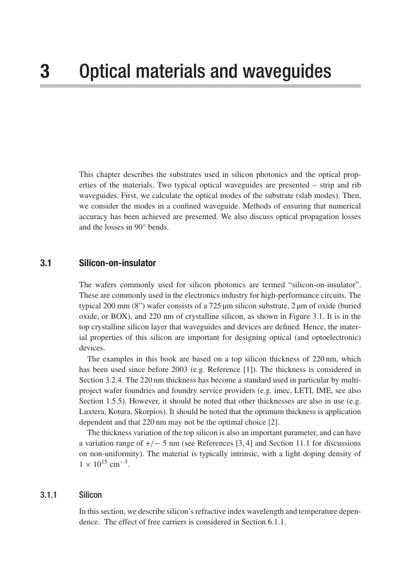
Image of the first page of this content. For PDF version, please use the ‘Save PDF’ preceeding this image.'
Type
Chapter
Information
Silicon Photonics Design
From Devices to Systems
, pp. 49 - 91
Publisher: Cambridge University Press
Print publication year: 2015

Access options

Get access to the full version of this content by using one of the access options below. (Log in options will check for institutional or personal access. Content may require purchase if you do not have access.)

References

[1]Dirk, Taillaert, Harold, Chong, Peter I., Borel, et al. “A compact two-dimensional grating coupler used as a polarization splitter”. IEEE Photonics Technology Letters 15.9 (2003), pp. 1249–1251 (cit. on p. 49).Google Scholar
[2]Dan-Xia, Xu, J. H., Schmid, G. T., Reed, et al. “Silicon Photonic Integration Platform – Have We Found The Sweet Spot?”. IEEE Journal of Selected Topics in Quantum Electronics 20.4 (2014), pp. 1–17. issn: 1077-260X. DOI: 10.1109/JSTQE.2014.2299634 (cit. on p. 49).Google Scholar
[3]W. A., Zortman, D. C., Trotter, and M. R., Watts. “Silicon photonics manufacturing”. Optics Express 18.23 (2010), pp. 23598–23607 (cit. on p. 49).Google Scholar
[4] A. V., Krishnamoorthy, Xuezhe, Zheng, GuoliangLi, Li, et al. “Exploiting CMOS manufacturing to reduce tuning requirements for resonant optical devices”. IEEE Photonics Journal 3.3 (2011), pp. 567–579. DOI: 10.1109/JPHOT.2011.2140367 (cit. on p. 49).Google Scholar
[5] Edward, Palik. Handbook of Optical Constants of Solids. Elsevier, 1998 (cit. on p. 50).Google Scholar
[6] Kurt, Oughstun and Natalie, Cartwright. “On the Lorentz–Lorenz formula and the Lorentz model of dielectric dispersion”. Optics Express 11 (2003), pp. 1541–1546 (cit. on p. 50).Google Scholar
[7] Lorenzo, Pavesi and Gérard, Guillot. Optical Interconnects: The Silicon Approach. 978-3-540-28910-4. Springer Berlin/Heidelberg, 2006 (cit. on p. 50).Google Scholar
[8] G., Cocorullo and I., Rendina. “Thermo-optical modulation at 1.5 μm in silicon etalon”. Electronics Letters 28.1 (1992), pp. 83–85. DOI: 10.1049/el:19920051 (cit. on p. 51).Google Scholar
[9] J. A., McCaulley, V. M., Donnelly, M., Vernon, and I., Taha. “Temperature dependence of the near-infrared refractive index of silicon, gallium arsenide, and indium phosphide”. Physical Review B 49.11 (1994), p. 7408 (cit. on p. 51).Google Scholar
[10] Pieter, Dumon. “Ultra-compact integrated optical filters in silicon-on-insulator by means of wafer-scale technology”. PhD thesis. Gent University, 2007 (cit. on p. 51).
[11] Bradley J., Frey, Douglas B., Leviton, and Timothy J., Madison. “Temperature-dependent refractive index of silicon and germanium”. Proceedings SPIE. Vol. 6273. 2006, 62732J–62732J–10. DOI: 10.1117/12.672850 (cit. on p. 51).Google Scholar
[12] Muzammil, Iqbal, Martin A., Gleeson, Bradley, Spaugh, et al. “Label-free biosensor arrays based on silicon ring resonators and high-speed optical scanning instrumentation”. IEEE Journal of Selected Topics in Quantum Electronics 16.3 (2010), pp. 654–661 (cit. on p. 52).Google Scholar
[13] Lukas, Chrostowski, Samantha, Grist, Jonas, Flueckiger, et al. “Silicon photonic resonator sensors and devices”. Proceedings of SPIE Volume 8236; Laser Resonators, Microresonators, and Beam Control XIV (Jan. 2012) (cit. on p. 52).
[14] Xu, Wang, Samantha, Grist, Jonas, Flueckiger, Nicolas A. F., Jaeger, and Lukas, Chrostowski. “Silicon photonic slot waveguide Bragg gratings and resonators”. Optics Express 21 (2013), pp. 19029–19039 (cit. on p. 52).Google Scholar
[15] Xu, Wang. “Silicon photonic waveguide Bragg gratings”. PhD thesis. University of British Columbia, 2013 (cit. on p. 54).
[16] Effective Mode Area – FDTD Solutions Knowledge Base. [Accessed 2014/04/14]. URL: http://docs.lumerical.com/en/fdtd/user_guide_effective_mode_area.html (cit. on p. 61).
[17] A., Densmore, D. X., Xu, P., Waldron, et al. “A silicon-on-insulator photonic wire based evanescent field sensor”. IEEE Photonics Technology Letters 18.23 (2006), pp. 2520–2522 (cit. on p. 61).Google Scholar
[18] D. X., Xu, A., Delge, J. H., Schmid, et al. “Selecting the polarization in silicon photonic wire components”. Proceedings of SPIE. Vol. 8266 (2012), 82660G (cit. on p. 61).Google Scholar
[19] N., Rouger, L., Chrostowski, and R., Vafaei. “Temperature effects on silicon-on-insulator (SOI) racetrack resonators: a coupled analytic and 2-D finite difference approach”. Journal of Lightwave Technology 28.9 (2010), pp. 1380–1391. DOI: 10.1109/JLT.2010.2041528 (cit. on p. 68).Google Scholar
[20] K. P., Yap, J.|Lapointe, B., Lamontagne, et al. “SOI waveguide fabrication process development using star coupler scattering loss measurements”. Proceedings Device and Process Technologies for Microelectronics, MEMS, Photonics, and Nanotechnology IV, SPIE (2008), p. 680014 (cit. on p. 69).Google Scholar
[21] Dietrich, Marcuse. Theory of Dielectric Optical Waveguides. Elsevier, 1974 (cit. on p. 69).Google Scholar
[22] F. P., Payne and J. P. R., Lacey. “A theoretical analysis of scattering loss from planar optical waveguides”. Optical and Quantum Electronics 26.10 (1994), pp. 977–986 (cit. on p. 69).Google Scholar
[23] Christopher G., Poulton, Christian, Koos, Masafumi, Fujii, et al. “Radiation modes and roughness loss in high index-contrast waveguides”. IEEE Journal of Selected Topics in Quantum Electronics 12.6 (2006), pp. 1306–1321 (cit. on p. 69).Google Scholar
[24] Frdric, Grillot, Laurent, Vivien, Suzanne, Laval, and Eric, Cassan. “Propagation loss in single-mode ultrasmall square silicon-on-insulator optical waveguides”. Journal of Lightwave Technology 24.2 (2006), p. 891 (cit. on p. 69).Google Scholar
[25] Tom, Baehr-Jones, Michael, Hochberg, and Axel, Scherer. “Photodetection in silicon beyond the band edge with surface states”. Optics Express 16.3 (2008), pp. 1659–1668 (cit. on p. 69).Google Scholar
[26] Jason J., Ackert, Abdullah S., Karar, John C., Cartledge, Paul E., Jessop, and Andrew P., Knights. “Monolithic silicon waveguide photodiode utilizing surface-state absorption and operating at 10 Gb/s”. Optics Express 22.9 (2014), pp. 10710–10715 (cit. on p. 69).Google Scholar
[27] A. D., Simard, N., Ayotte, Y., Painchaud, S., Bedard, and S., LaRochelle. “Impact of sidewall roughness on integrated Bragg gratings”. Journal of Lightwave Technology 29.24 (2011), pp. 3693–3704 (cit. on p. 69).Google Scholar
[28] Po, Dong, Wei, Qian, Shirong, Liao, et al. “Low loss shallow-ridge silicon waveguides”. Optics Express 18.14 (2010), pp. 14474–14479 (cit. on p. 69).Google Scholar
[29] Yurii, Vlasov and Sharee, McNab. “Losses in single-mode silicon-on-insulator strip waveguides and bends”. Optics Express 12.8 (2004), pp. 1622–1631. DOI: 10.1364/OPEX.12.001622 (cit. on p. 70).Google Scholar
[30] Guoliang, Li, Jin, Yao, Hiren, Thacker, et al. “Ultralow-loss, high-density SOI optical waveguide routing for macrochip interconnects”. Optics Express 20.11 (May 2012), pp. 12035–12039. DOI: 10.1364/OE.20.012035 (cit. on p. 70).Google Scholar
[31] Wim, Bogaerts, Pieter, Dumon, et al. “Compact wavelength-selective functions in silicon-on-insulator photonic wires”. IEEE Journal of Selected Topics in Quantum Electronics 12.6 (2006) (cit. on p. 70).Google Scholar
[32] Tom, Baehr-Jones, Ran, Ding, Ali, Ayazi, et al. “A 25 Gb/s silicon photonics platform”. arXiv:1203.0767v1 (2012) (cit. on pp. 71, 72).Google Scholar
[33] Using Mode Expansion Monitors – FDTD Solutions Knowledge Base. [Accessed 2014/04/14]. URL: http://docs.lumerical.com/en/fdtd/user_guide_using_mode_expansion_monitors.html (cit. on p. 73).
[34] R. J., Bojko, J., Li, L., He, et al. “Electron beam lithography writing strategies for low loss, high confinement silicon optical waveguides”. Journal of Vacuum Science & Technology B: Microelectronics and Nanometer Structures 29.6 (2011), 06F309–06F309 (cit. on p. 73).Google Scholar
[35] Bent Waveguide Calculation – MODE Solutions Knowledge Base. [Accessed 2014/04/14]. URL: http://docs.lumerical.com/en/mode/usr_waveguide_bend.html (cit. on p. 75).
[36] Amnon, Yariv and Pochi, Yeh. Photonics: Optical Electronics in Modern Communications (The Oxford Series in Electrical and Computer Engineering). Oxford University Press, Inc., 2006 (cit. on pp. 77, 78).Google Scholar

Save book to Kindle

To save this book to your Kindle, first ensure coreplatform@cambridge.org is added to your Approved Personal Document E-mail List under your Personal Document Settings on the Manage Your Content and Devices page of your Amazon account. Then enter the ‘name’ part of your Kindle email address below. Find out more about saving to your Kindle.

Note you can select to save to either the @free.kindle.com or @kindle.com variations. ‘@free.kindle.com’ emails are free but can only be saved to your device when it is connected to wi-fi. ‘@kindle.com’ emails can be delivered even when you are not connected to wi-fi, but note that service fees apply.

Find out more about the Kindle Personal Document Service.

Available formats
×

Save book to Dropbox

To save content items to your account, please confirm that you agree to abide by our usage policies. If this is the first time you use this feature, you will be asked to authorise Cambridge Core to connect with your account. Find out more about saving content to Dropbox.

Available formats
×

Save book to Google Drive

To save content items to your account, please confirm that you agree to abide by our usage policies. If this is the first time you use this feature, you will be asked to authorise Cambridge Core to connect with your account. Find out more about saving content to Google Drive.

Available formats
×