Skip to main content Accessibility help
×
Hostname: page-component-77c89778f8-cnmwb Total loading time: 0 Render date: 2024-07-21T08:30:27.352Z Has data issue: false hasContentIssue false

12 - Testing and packaging

from Part IV - System design

Published online by Cambridge University Press:  05 April 2015

Lukas Chrostowski
Affiliation:
University of British Columbia, Vancouver
Michael Hochberg
Affiliation:
Coriant Advanced Technology Group
Get access

Summary

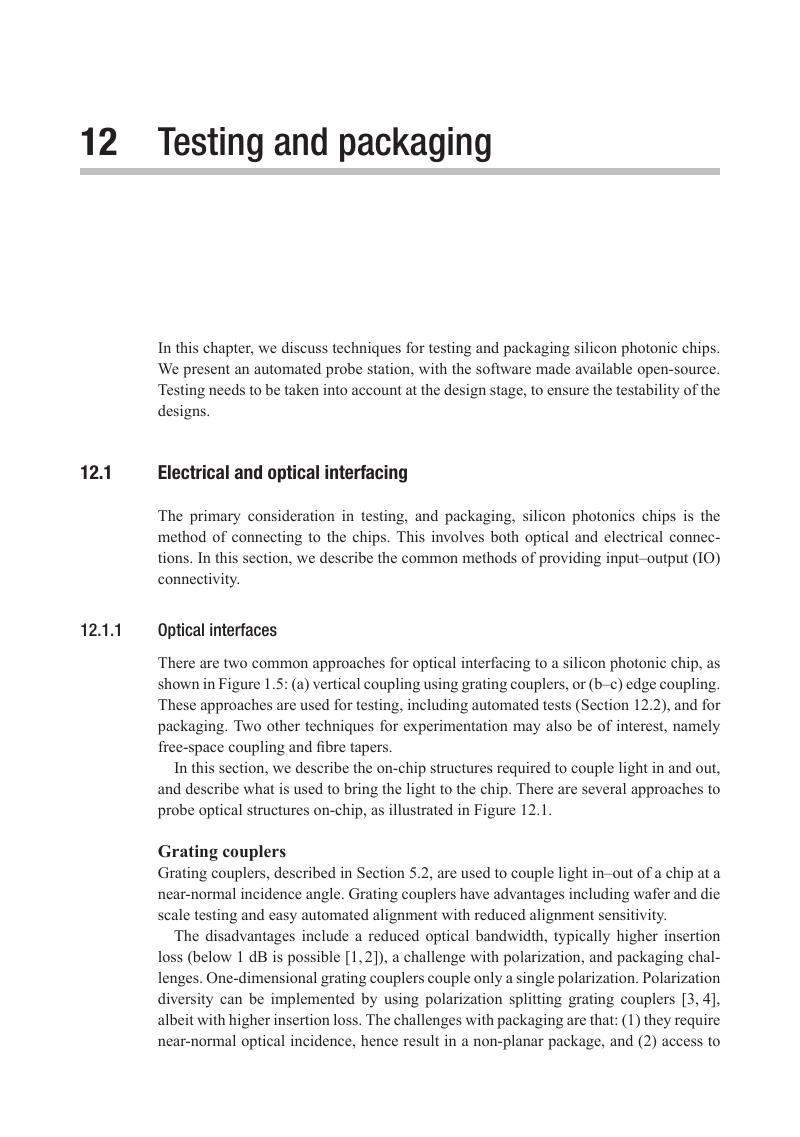
Image of the first page of this content. For PDF version, please use the ‘Save PDF’ preceeding this image.'
Type
Chapter
Information
Silicon Photonics Design
From Devices to Systems
, pp. 381 - 405
Publisher: Cambridge University Press
Print publication year: 2015

Access options

Get access to the full version of this content by using one of the access options below. (Log in options will check for institutional or personal access. Content may require purchase if you do not have access.)

References

[1] A., Mekis, S., Abdalla, D., Foltz, et al. “A CMOS photonics platform for high-speed optical interconnects”. Photonics Conference (IPC). IEEE. 2012, pp. 356–357 (cit. on p. 381).Google Scholar
[2] Wissem Sfar, Zaoui, Andreas, Kunze, Wolfgang, Vogel, et al. “Bridging the gap between optical fibers and silicon photonic integrated circuits”. Optics Express 22.2 (2014), pp. 1277–1286. DOI: 10.1364/OE.22.001277 (cit. on p. 381).Google Scholar
[3] Dirk, Taillaert, Harold, Chong, Peter I., Borel, et al. “A compact two-dimensional grating coupler used as a polarization splitter”. IEEE Photonics Technology Letters 15.9 (2003), pp. 1249–1251 (cit. on p. 381).Google Scholar
[4] A., Mekis, S., Gloeckner, G., Masini, et al. “A grating-coupler-enabled CMOS photonics platform”. IEEE Journal of Selected Topics in Quantum Electronics 17.3 (2011), pp. 597–608. DOI: 10.1109/JSTQE.2010.2086049 (cit. on pp. 381, 385, 389).Google Scholar
[5] Bradley W., Snyder and Peter A., O'Brien. “Developments in packaging and integration for silicon photonics”. Proc. SPIE. Vol. 8614. 2013, pp. 86140D'86140D–9. DOI: 10.1117/12.2012735 (cit. on pp. 382, 383, 385, 389).Google Scholar
[6] Na, Fang, Zhifeng, Yang, Aimin, Wu, et al. “Three-dimensional tapered spot-size converter based on (111) silicon-on-insulator”. IEEE Photonics Technology Letters 21.12 (2009), pp. 820–822 (cit. on p. 382).Google Scholar
[7] Minhao, Pu, Liu, Liu, Haiyan, Ou, Kresten, Yvind, and Jorn M., Hvam. “Ultra-low-loss inverted taper coupler for silicon-on-insulator ridge waveguide”. Optics Communications 283.19 (2010), pp. 3678–3682 (cit. on p. 382).Google Scholar
[8] M. R., Watts, H. A., Haus, and E. P., Ippen. “Integrated mode-evolution-based polarization splitter”. Optics Letters 30.9 (2005), pp. 967–969 (cit. on p. 382).Google Scholar
[9] Daoxin, Dai and John E., Bowers. “Novel concept for ultracompact polarization splitter-rotator based on silicon nanowires”. Optics Express 19.11 (2011), pp. 10940–10949 (cit. on p. 382).Google Scholar
[10] Han, Yun. “Design and characterization of a dumbbell micro-ring resonator reflector”. MA thesis. 2013. URL: https://circle.ubc.ca/handle/2429/44535 (cit. on p. 382).
[11] Charlie, Lin. “Photonic device design flow: from mask layout to device measurement”. MA thesis. 2012. URL: https://circle.ubc.ca/handle/2429/43510 (cit. on pp. 382, 385).
[12] PLC Connections PLCC – Silicon Photonics. [Accessed 2014/04/14]. URL: http://www.plcconnections.com/silicon.html (cit. on pp. 383, 384, 385).
[13] Y., Painchaud, M., Poulin, F., Pelletier, et al. “Silicon-based products and solutions”. Proc. SPIE. 2014 (cit. on pp. 383, 389).Google Scholar
[14] F. E., Doany, B. G., Lee, et al. IEEE Journal of Lightwave Technology 29.475 (2011) (cit. on p. 383).
[15] T., Barwicz, Y., Taira, “Low-Cost Interfacing of Fibers to Nanophotonic Waveguides: Design for Fabrication and Assembly Tolerances”, IEEE Photonics Journal, Vol. 6, no. 4, 6600818, 2014, DOI: 10.1109/JPHOT.2014.2331251 (cit. on p. 383).Google Scholar
[16] Tom, Baehr-Jones, Ran, Ding, Ali, Ayazi, et al. “A 25 Gb/s silicon photonics platform”. arXiv:1203.0767v1 (2012) (cit. on p. 385).Google Scholar
[17] Amit, Khanna, Youssef, Drissi, Pieter, Dumon, et al. “ePIX-fab: the silicon photonics platform”. SPIE Microtechnologies. International Society for Optics and Photonics. 2013, 87670H (cit. on p. 385).Google Scholar
[18] Ellen, Schelew, Georg W., Rieger, and Jeff F., Young. “Characterization of integrated planar photonic crystal circuits fabricated by a CMOS foundry”. Journal of Lightwave Technology 31.2 (2013), pp. 239–248 (cit. on p. 385).Google Scholar
[19] Muzammil, Iqbal, Martin A, Gleeson, Bradley, Spaugh, et al. “Label-free biosensor arrays based on silicon ring resonators and high-speed optical scanning instrumentation”. IEEE Journal of Selected Topics in Quantum Electronics 16.3 (2010), pp. 654–661 (cit. onp. 385).Google Scholar
[20] S., Janz, D.-X., Xu, M., Vachon, et al. “Photonic wire biosensor microarray chip and instrumentation with application to serotyping of Escherichia coli isolates”. Optics Express 21.4 (2013), pp. 4623–1637 (cit. on p. 385).Google Scholar
[21] Paul E., Barclay, Kartik, Srinivasan, Matthew, Borselli, and Oskar, Painter. “Probing the dispersive and spatial properties of photonic crystal waveguides via highly efficient coupling from fiber tapers”. Applied Physics Letters 85.1 (2004), pp. 4–6 (cit. on p. 386).Google Scholar
[22] J. C., Knight, G., Cheung, F., Jacques, and T. A., Birks. “Phase-matched excitation of whispering-gallery-mode resonances by a fiber taper”. Optics Letters 22.15 (1997), pp. 1129–1131 (cit. onp. 386).Google Scholar
[23] C. P., Michael, M., Borselli, T. J., Johnson, C., Chrystal, and O., Painter. “An optical fiber-taper probe for wafer-scale microphotonic device characterization”. arXiv preprint physics/0702079 (2007) (cit. on p. 386).Google Scholar
[24] Probe Tips – Signatone. [Accessed 2014/04/14]. URL: http://www.signatone.com/products/tipsholders/ (cit. on p. 387).
[25] S-725 Micropositioner – Signatone. [Accessed 2014/04/14]. URL: http://www.signatone.com/products/micropositioners/s725.asp (cit. on p. 387).
[26] Welcome to Cascade Microtech: Cascade Microtech Inc. [Accessed 2014/04/14]. URL: http://www.cmicro.com (cit. on p. 387).
[27] Technoprobe – Advanced Wafer Probe Cards. [Accessed 2014/04/14]. URL: http://www.technoprobe.com (cit. on p. 387).
[28] Cascade, Microtech. Application Note: Mechanical Layout Rules for Infinity Probes. [Accessed 2014/04/14]. URL: http://www.cmicro.com/file/mechanical-layout-rules-for-infinity-probes (cit. on p. 388).
[29] West-Bond, Inc., Home Page – Wire Bonders, Wire Bonding. [Accessed 2014/04/14]. URL: http://www.westbond.com/ (cit. on p. 388).
[30] Advanced Design System (ADS) – Agilent. [Accessed 2014/04/14]. URL: http://www.home.agilent.com/en/pc-1297113/advanced-design-system-ads (cit. onp. 388).
[31] Fu-Yi, Han, Kung-Chung, Lu, Tzyy-Sheng, Horng, et al. “Packaging effects on the figure of merit of a CMOS cascode low-noise amplifier: flip-chip versus wire-bond”. Microwave Symposium Digest, 2009. MTT'09. IEEE MTT-S International. IEEE. 2009, pp. 601–604 (cit. on p. 389).Google Scholar
[32] 3D-IC Design and Test Solutions – Mentor Graphics. [Accessed 2014/04/14]. URL: http://www.mentor.com/solutions/3d-ic-design (cit. on p. 389).
[33] Richard K., Ulrich and William D., Brown. Advanced Electronic Packaging. Wiley-Interscience/IEEE, 2006 (cit. on p. 389).Google Scholar
[34] Andrea, Chen and Randy, Lo. Semiconductor Packaging: Materials Interaction and Reliability. CRC Press, 2012 (cit. on p. 389).Google Scholar
[35] Peter De, Dobbelaere, Ali, Ayazi, Yuemeng, Chi, et al. “Packaging of silicon photonics systems”. Optical Fiber Communication Conference. Optical Society of America. 2014, W3I–2 (cit. on p. 389).Google Scholar
[36] Automated Probe Station – siepic.ubc.ca. [Accessed 2014/04/14]. URL: http://siepic.ubc.ca/probestation (cit. on pp. 389, 393).
[37] T., Baehr-Jones, R., Ding, Y., Liu, et al. “Ultralow drive voltage silicon traveling-wave modulator”. Optics Express 20.11 (2012), pp. 12 014–12 020 (cit. on p. 400).Google Scholar
[38] J. J., Ackert, J. K., Doylend, D. F., Logan, et al. “Defect-mediated resonance shift of silicon-on-insulator racetrack resonators”. Optics Express 19.13 (2011), pp. 11 969–11 976. DOI: 10.1364/OE.19.011969 (cit. on p. 400).Google Scholar

Save book to Kindle

To save this book to your Kindle, first ensure coreplatform@cambridge.org is added to your Approved Personal Document E-mail List under your Personal Document Settings on the Manage Your Content and Devices page of your Amazon account. Then enter the ‘name’ part of your Kindle email address below. Find out more about saving to your Kindle.

Note you can select to save to either the @free.kindle.com or @kindle.com variations. ‘@free.kindle.com’ emails are free but can only be saved to your device when it is connected to wi-fi. ‘@kindle.com’ emails can be delivered even when you are not connected to wi-fi, but note that service fees apply.

Find out more about the Kindle Personal Document Service.

Available formats
×

Save book to Dropbox

To save content items to your account, please confirm that you agree to abide by our usage policies. If this is the first time you use this feature, you will be asked to authorise Cambridge Core to connect with your account. Find out more about saving content to Dropbox.

Available formats
×

Save book to Google Drive

To save content items to your account, please confirm that you agree to abide by our usage policies. If this is the first time you use this feature, you will be asked to authorise Cambridge Core to connect with your account. Find out more about saving content to Google Drive.

Available formats
×