Skip to main content Accessibility help
×
Hostname: page-component-77c89778f8-n9wrp Total loading time: 0 Render date: 2024-07-21T10:28:32.635Z Has data issue: false hasContentIssue false

7 - Detectors

from Part III - Active Components

Published online by Cambridge University Press:  05 April 2015

Lukas Chrostowski
Affiliation:
University of British Columbia, Vancouver
Michael Hochberg
Affiliation:
Coriant Advanced Technology Group
Get access

Summary

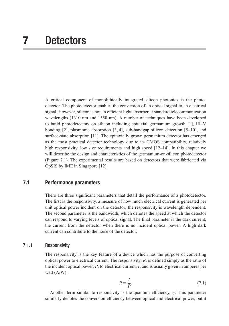
Image of the first page of this content. For PDF version, please use the ‘Save PDF’ preceeding this image.'
Type
Chapter
Information
Silicon Photonics Design
From Devices to Systems
, pp. 259 - 294
Publisher: Cambridge University Press
Print publication year: 2015

Access options

Get access to the full version of this content by using one of the access options below. (Log in options will check for institutional or personal access. Content may require purchase if you do not have access.)

References

[1] L., Colace. G., Masini, F., Galluzzi. et al. “Metal–semiconductor–metal near-infrared light detector based on epitaxial Ge/Si”. Applied Physics Letters 72.24 (1998), pp. 3175–3177 (cit. on pp. 259, 264, 265).Google Scholar
[2] Hsu-Hao, Chang, Ying-hao, Kuo, Richard, Jones, Assia, Barkai, and John E., Bowers. “Integrated hybrid silicon triplexer”. Optics Express 18.23 (2010), pp. 23 891–23 899 (cit. on p 259).Google Scholar
[3] Ilya, Goykhman, Boris, Desiatov, Jacob, Khurgin, Joseph, Shappir, and Uriel, Levy. “Locally oxidized silicon surface-plasmon Schottky detector for telecom regime”. Nano Letters 11.6 (2011), pp. 2219–2224 (cit. on pp. 259, 264).Google Scholar
[4] Ilya, Goykhman, Boris, Desiatov, Jacob, Khurgin, Joseph, Shappir, and Uriel, Levy. “Wave-guide based compact silicon Schottky photodetector with enhanced responsivity in the telecom spectral band”. Optics Express 20.27 (2012), pp. 28 594–28 602 (cit. on pp. 259, 264).Google Scholar
[5] J. D. B, Bradley, P. E., Jessop. and A. P., Knights. “Silicon waveguide-integrated optical power monitor with enhanced sensitivity at 1550 nm”. Applied Physics Letters 86.24 (2005), pp. 241 103–241 103 (cit. on pp. 259, 264).Google Scholar
[6] A. P., Knights. J. D. B., Bradley. S. H., Gou. and P. E., Jessop. “Silicon-on-insulator waveguide photodetector with self-ion-implantation-engineered-enhanced infrared response”. Journal of Vacuum Science & Technology A 24.3 (2006), pp. 783–786 (cit. on pp. 259, 264).Google Scholar
[7] M. W., Geis. S. J., Spector. M. E., Grein. et al. “Silicon waveguide infrared photodiodes with >35 GHz bandwidth and phototransistors with 50 AW-1 response”. Optics Express 17.7 (2009), pp. 5193–5204. DOI: 10.1364/OE.17.005193 (cit. on pp. 259, 264).Google Scholar
[8] J. K., Doylend. P. E., Jessop. and A. P., Knights. “Silicon photonic resonator-enhanced defect-mediated photodiode for sub-bandgap detection”. Optics Express 18.14 (2010), pp. 14 671–14 678 (cit. on pp. 259, 264).Google Scholar
[9] Jason J., Ackert. Abdullah S., Karar. Dixon J., Paez. et al. “10 Gbps silicon waveguide-integrated infrared avalanche photodiode”. Optics Express 21.17 (2013), pp. 19 530–19 537. DOI: 10.1364/OE.21.019530 (cit. on pp. 259, 264).Google Scholar
[10] Richard R., Grote. Kishore, Padmaraju, Brian, Souhan, et al. “10 Gb/s Error-free operation of all-silicon ion-implanted-waveguide photodiodes at 1.55”. IEEE Photonics Technology Letters 25.1 (2013), pp. 67–70 (cit. on pp. 259, 264).Google Scholar
[11] Jason J., Ackert. Abdullah S., Karar. John C., Cartledge. Paul E., Jessop. and Andrew P., Knights. “Monolithic silicon waveguide photodiode utilizing surface-state absorption and operating at 10 Gb/s”. Optics Express 22.9 (2014), pp. 10710–10715 (cit. on p. 259).Google Scholar
[12] Tsung-Yang, Liow, Kah-Wee, Ang, Qing, Fang, et al. “Silicon modulators and germanium photodetectors on SOI: monolithic integration, compatibility, and performance optimization”. IEEE Journal of Selected Topics in Quantum Electronics 16.1 (2010), pp. 307–315 (cit. on pp. 259, 276, 280, 281).Google Scholar
[13] R., Ichikawa. S., Takita, Y., Ishikawa. and K., Wada. “Germanium as a material to enable silicon photonics”. Silicon Photonics II. Ed. by David J., Lockwood and Lorenzo, Pavesi. Vol. 119. Topics in Applied Physics. Springer Berlin Heidelberg, 2011, pp. 131–141. ISBN: 978-3-642-10505-0. DOI: 10.1007/978-3-642-10506-7 5 (cit. on p. 259).Google Scholar
[14] Ari, Novack, Mike, Gould, Yisu, Yang, et al. “Germanium photodetector with 60 GHz bandwidth using inductive gain peaking”. Optics Express 21.23 (2013), pp. 28 387–28 393. DOI: 10.1364/OE.21.028387 (cit. on pp. 259, 275).Google Scholar
[15] M. C., Teich and B. E. A., Saleh. Fundamentals of Photonics. Canada, Wiley Interscience (1991), p. 3 (cit. on pp. 260, 268).Google Scholar
[16] S. M., Sze and K. K., Ng. Physics of Semiconductor Devices. Wiley Interscience, 2006 (cit. on p. 261).Google Scholar
[17] Sheila, Prasad, Hermann, Schumacher, and Anand, Gopinath. High-speed Electronics and Optoelectronics: Devices and Circuits. Cambridge University Press, 2009 (cit. on p. 261).Google Scholar
[18] L., Vivien. A., Polzer, D., Marris-Morini, et al. “Zero-bias 40Gbit/s germanium waveguide photodetector on silicon”. Optics Express 20 (2012), pp. 1096–1101. DOI: 10.1364/OE.20.001096 (cit. on pp. 262, 272).Google Scholar
[19] Kah-Wee, Ang, Joseph, Weisheng Ng, Guo-Qiang, Lo, and Dim-Lee, Kwong. “Impact of field-enhanced band-traps-band tunneling on the dark current generation in germanium pin photodetector”. Applied Physics Letters 94.22 (2009), p. 223 515 (cit. on p. 262).Google Scholar
[20] Mitsuru, Takenaka, Kiyohito, Morii, Masakazu, Sugiyama, Yoshiaki, Nakano, and Shinichi, Takagi. “Dark current reduction of Ge photodetector by GeO2 surface passivation and gas-phase doping”. Optics Express 20.8 (2012), pp. 8718–8725 (cit. on p. 263).Google Scholar
[21] Edward, Palik. Handbook of Optical Constants of Solids. Elsevier, 1998 (cit. on p. 265).Google Scholar
[22] A. P., Knights. D. F., Logan. P. E., Jessop. et al. “Deep-levels in silicon waveguides: a route to monolithic integration”. Photonics Conference (PHO), 2011 IEEE. IEEE. 2011, pp. 461–462 (cit. on p. 264).Google Scholar
[23] Alexander W., Fang. Richard, Jones, Hyundai, Park, et al. “Integrated AlGaInAs-silicon evanescent racetrack laser and photodetector”. Optics East 2007. International Society for Optics and Photonics. 2007, 67750P (cit. on p. 264).Google Scholar
[24] Govind P, Agrawal. Fiber-optic Communication Systems. Vol. 1. 1997 (cit. on p. 267).
[25] Tom, Baehr-Jones, Ran, Ding, Ali, Ayazi, et al. “A 25 Gb/s silicon photonics platform”. arXiv:1203.0767v1 (2012) (cit. on p. 267).Google Scholar
[26] Amit, Khanna, Youssef, Drissi, Pieter, Dumon, et al. “ePIX-fab: the silicon photonics platform”. SPIE Microtechnologies. International Society for Optics and Photonics. 2013, 87670H (cit. on p. 267).Google Scholar
[27] A., Mekis. S., Abdalla, D., Foltz. et al. “A CMOS photonics platform for high-speed optical interconnects”. Photonics Conference (IPC). IEEE. 2012, pp. 356–357 (cit. on p. 267).Google Scholar
[28] Yi, Zhou, Masaaki, Ogawa, Xinhai, Han, and Kang L., Wang. “Alleviation of Fermi-level pinning effect on metal/germanium interface by insertion of an ultrathin aluminum oxide”. Applied Physics Letters 93.20 (2008), p. 202105 (cit. on p. 274).Google Scholar
[29] A., Dimoulas. P., Tsipas, A., Sotiropoulos. and E. K., Evangelou. “Fermi-level pinning and charge neutrality level in germanium”. Applied Physics Letters 89.25 (2006), p. 252110 (cit. on p. 274).Google Scholar
[30] R. R., Lieten. V. V., Afanasev. N. H., Thoan. et al. “Mechanisms of Schottky barrier control on n-type germanium using Ge3N4 interlayers”. Journal of the Electrochemical Society 158.4 (2011), H358–H362 (cit. on p. 274).Google Scholar
[31] Y., Painchaud. M., Poulin, F., Pelletier. et al. “Silicon-based products and solutions”. Proc. SPIE. 2014 (cit. on p. 275).Google Scholar

Save book to Kindle

To save this book to your Kindle, first ensure coreplatform@cambridge.org is added to your Approved Personal Document E-mail List under your Personal Document Settings on the Manage Your Content and Devices page of your Amazon account. Then enter the ‘name’ part of your Kindle email address below. Find out more about saving to your Kindle.

Note you can select to save to either the @free.kindle.com or @kindle.com variations. ‘@free.kindle.com’ emails are free but can only be saved to your device when it is connected to wi-fi. ‘@kindle.com’ emails can be delivered even when you are not connected to wi-fi, but note that service fees apply.

Find out more about the Kindle Personal Document Service.

  • Detectors
  • Lukas Chrostowski, University of British Columbia, Vancouver, Michael Hochberg
  • Book: Silicon Photonics Design
  • Online publication: 05 April 2015
  • Chapter DOI: https://doi.org/10.1017/CBO9781316084168.008
Available formats
×

Save book to Dropbox

To save content items to your account, please confirm that you agree to abide by our usage policies. If this is the first time you use this feature, you will be asked to authorise Cambridge Core to connect with your account. Find out more about saving content to Dropbox.

  • Detectors
  • Lukas Chrostowski, University of British Columbia, Vancouver, Michael Hochberg
  • Book: Silicon Photonics Design
  • Online publication: 05 April 2015
  • Chapter DOI: https://doi.org/10.1017/CBO9781316084168.008
Available formats
×

Save book to Google Drive

To save content items to your account, please confirm that you agree to abide by our usage policies. If this is the first time you use this feature, you will be asked to authorise Cambridge Core to connect with your account. Find out more about saving content to Google Drive.

  • Detectors
  • Lukas Chrostowski, University of British Columbia, Vancouver, Michael Hochberg
  • Book: Silicon Photonics Design
  • Online publication: 05 April 2015
  • Chapter DOI: https://doi.org/10.1017/CBO9781316084168.008
Available formats
×